Altium today announced plans to acquire Morfik Technology, a provider of cloud-based software applications, in an all-stock transaction worth an estimated AU$3.3 million. The deal is pending due diligence. Within the next fiscal year, there will be no significant impact on Altium's revenues.
PRINTED CIRCUIT DESIGN & FAB spoke with Altium’s Alan Smith this morning:
Altium's Alan Smith
PCDF: How many employees does Morfik have? How many are software designers?
AS: Twelve in total, nine of which are software developers.
PCDF: When is the deal scheduled to close?
AS: We expect this to be in the next few weeks, but we can't be precise because of the due diligence that forms part of the process. Having said that, we are also accelerating the acquisition by bringing the Morfik development team into Altium's offices to work with the Altium team on the development of the ecosystem infrastructure that we now plan to build into our software.
PCDF: What specifically made Morfik so attractive to Altium?
AS: Altium has been working with Morfik for a number of years, so Morfik's attraction, based on what it has done with the development of tools to create dynamic cloud-based ecosystems, is well understood. It has to do with Morfik's software engineering approach to the creation of object-oriented connectivity to the Internet. The two key phrases here are dynamic and object-oriented. These are essential for managing large amounts of content, which is what you have in electronics design: content down to the scale of individual components.
PCDF: What are the top technical challenges behind moving electronics design to cloud-based architectures, and how does the Morfik acquisition help Altium overcome them?
AS: Two points: 1) Tactical: helping Altium establish its ecosystem today for subscription-based content delivery. 2) Longer term: Morfik is about developing cloud-based applications; these are the applications that will be the highest layer, running on the “sea of connected devices” in this ecosystem. If we are to deliver the tools and solution to help the designer move from device design to ecosystem design, then cloud-application development is a fundamental part of this solution.
PCDF: When it comes to cloud computing, Altium is on record as seeing Google as being superior to Microsoft. Will *customers* have to choose a platform based on one or the other, or will electronics design in the cloud be platform-independent?
AS: We don’t really know. Amazon (Amazon Web Services) is more significant than either Google or Microsoft because it provides a much broader industrial-scale infrastructure for cloud-based application that is provided as a utility service for organizations that want to provide these kinds of solutions.
PCDF: Would a cloud-based infrastructure force any change to the subscription model that most ECAD companies now rely on?
AS: Not specifically. Cloud-based (Internet-based) models allow a real-time connection between customers and suppliers, as well as between customers and customers. This creates the possibility of having a much stronger and timelier value exchange between these parties. In the future, they can move the basis of software subscriptions away from being primarily based on software upgrades (new features, etc.) to a much stronger focus on content that can be delivered over time. In electronics design this includes component models, designs, price and availability from part suppliers, as well as feature upgrades being delivered in a “plug-in” model.
PCDF: Would cloud-based electronics design help resolve the persistent library and documentation issues that today cost designers extraordinary amounts of time?
AS: An emphatic yes. Vastly improved data management is already a big focus of the next release of Altium Designer, in Beta today, and cloud-based data exchange is a big part of this. Initial focus is on management of data between the board-design process, and the fabricators and assemblers of those boards, especially when the parties are in different regions and speak different languages.
Author: Gregory Dripps; This email address is being protected from spambots. You need JavaScript enabled to view it.. Abstract: Asia is adopting core elements of REACH, although the region is not adopting the regulation itself. Registration and reporting are based on tonnage bands, with mandated testing requirements (physical/chemical plus toxicity). Possession of data packages will become a currency of the future as management controls consider a substance’s potential hazards and use, not just hazards. A philosophical shift is underway, whereby the notion that existing or new materials are safe is being abandoned, and comprehensive analysis and testing data are required to demonstrate an acceptable hazard profile. In many nations, rules will go into effect as early as this year. (IPC Symposium on Electronics and the Environment, July 2010)
“Recent Developments in the Implementation of the EU REACH Regulations”
Author: Michael Kirschner; mike@designchain-associates. Abstract: More than 140,000 substances have been preregistered, almost five times more than expected. To date, there are 38 candidate substances of very high concern (SVHC), and the Commission expects 165 by 2012. Until a listed substance is authorized or restricted, it remains a Candidate SVHC. To use an SVHC, make sure your supplier is legally authorized if your supply chain goes through the European Environment Agency. Furthermore, compliance in the EU does not mean compliance elsewhere. (IPC Symposium on Electronics and the Environment, July 2010)
“Halogen–Free: A Regulatory Overview”
Author: Susan Landry; This email address is being protected from spambots. You need JavaScript enabled to view it.. Abstract: Combustion gases generated during fires (whether or not flame retardants are present) that contribute to acute toxicity include CO, HCN, HCl, and acrolein. Carbon monoxide is responsible for more than 90% of all fire-related deaths. The most important pollutants generated in fires are polycyclic aromatic hydrocarbons (PAHs) and polyhalogenated dibenzodioxins and furans (PHDDs/PHDFs). Measurements made in large fires have shown that the PAHs have an up to 500 times higher cancer risk than the PHDDs/PHDFs. PAHs are generated in all fires, and many are carcinogenic compounds. In the US, the “Chemicals of Concern” Action List includes phthalates, short-chain chlorinated paraffins, polybrominated diphenyl ethers (PBDEs), and perfluorinated chemicals, including PFOA. An upcoming DfE will review Deca-BDE alternatives. The Department of Toxic Substances Control is called on to scientifically and systematically identify and prioritize chemicals and consumer products for manufacturers to conduct alternatives assessments, and DTSC could impose regulatory responses for alternatives selected by manufacturers. In June the European Parliament Environmental Committee voted to support amendments that require further evaluation instead of a ban on the use of certain organobrominated materials and PVC in electronics and electrical equipment, with certain exclusions for materials for military purposes and vehicles. (MEPs also called for a ban on nanosilver and carbon nanotubes, and that other EEE material containing nanomaterials should be labeled.) Amendments will now be considered by the full plenary session of the European Parliament. (IPC Symposium on Electronics and the Environment, July 2010)
Laminate Environmental Testing
“The Combustion Testing Phase EPA DfE Project on Flame Retardants for Circuit Boards”
Author: Dr. Emma Lavoie, et al; This email address is being protected from spambots. You need JavaScript enabled to view it.. Abstract: Goals of this work, a partnership of the US EPA and various industry suppliers, included identifying and characterizing commercially available flame retardants and their environmental, health, safety, and fate aspects in FR-4 printed circuit boards. The work applied lifecycle thinking to consider hazards and exposures, and used EPA New Chemicals Program criteria to evaluate hazard and environmental fate concerns. Methods included comparing the combustion byproducts from FR-4 laminates and PCB materials with different flame retardants during potential thermal end-of-life processes, including open burning, incineration, and smelting. Testing is designed to be a first step in providing industry with a comparative analysis of combustion byproducts from these materials, and to help inform further studies to better understand these byproducts in real-world scenarios. Investigations covered combustion testing of printed circuit board laminates, including materials containing phosphorus, TBBPA and no flame-retardant additives under temperatures of 300°, 700° and 900°C, with and without oxygen. (IPC Symposium on Electronics and the Environment, July 2010) CA
This column provides abstracts from recent industry conferences and company white papers. With the amount of information increasing, our goal is to provide an added opportunity for readers to keep abreast of technology and business trends.
Conferences around the world are buzzing over the growth projections for high brightness light-emitting diodes (HB LED). In Korea, almost 200 people attended the International LED and Green Lighting Seminar in June, while more than 20,000 people visited the colocated LED and OLED Expo. More than 200 people attended special sessions on LEDs during SemiCon West in San Francisco this past July. Companies are looking at the explosive industry growth, and all hope for a piece of the pie. Strategies Unlimited, Credit Suisse, and McKinsey predict that the LED market – driven by three major applications (general lighting, backlighting, and automotive) – will grow at a 40% CAGR through 2015.
According to the Optoelectronics Industry Development Association, three segments – automotive, lighting, and mobile applications – are expected to grow to 89% of all applications in 2021. What is driving the growth? In the case of lighting, much of the growth comes from pending bans on incandescent bulbs and government mandates that lighting be converted to LEDs for energy savings.
The technology to produce LED die is based on semiconductor diode technology. The emitted wavelength of light depends on the specific semiconductor material used. The key to producing high-quality LED die is the growth of the epitaxial layers and an active p-n junction on an optimum substrate. The p-n junction is critical in determining the device’s internal quantum efficiency (IQE), and the substrate is important because it should match the lattice constant of the semiconductor. The matching lattice constant helps reduce dislocation defects. Dislocation defects can adversely affect the performance of the LED.
Key tools for the growth of the epitaxial layers include MOCVD equipment. Wafers are typically two to four inches with a constant pressure to continue moving to larger wafer sizes.
The packaging and assembly process is also critical to the performance, reliability, and lifetime of the LED product. LED packaging tends to be nonstandard, with every package unique to the supplier.
LED packaging options include use of one large LED die in a package versus multiple die. Advantages and disadvantages are still being debated. It is not clear if one method will dominate or if both solutions will be used. In some cases, multiple die are mounted directly on a metal core substrate or on leadframes.
Thermal issues. Thermal issues have been reported to account for as much as 50% of the failures in lighting. Effectively removing this heat is critical to control junction temperatures of the LED chips, to ensure long device lifetimes, and to maintain the spectral and efficiency characteristics of the light source. Controlling the LED junction temperature (Tj) from 50° to 100°C is critical to LED performance. As the junction temperature (Tj) of the LED changes, the wavelength of emitted light shifts, making color control difficult. If Tj is excessively high, the active region of the LED and the electrodes of the device can degrade, leading to a decrease in the device light output. High Tj can also reduce LED life. Failure to effectively remove heat from the LED source can also degrade the phosphors in the LED package. as well as other packaging materials. Some examples of the latter are yellowing of the encapsulation material and higher absorption losses at reflective surfaces. Depending on the temperature changes, the coefficient of thermal expansion and glass transition temperature of these materials can lead to mechanical stresses that cause failure of the package or the LED die. If catastrophic failure does not occur, these effects often just reduce the lumens output of the package and thus the overall efficiency (lumens per watt) of the source. Excess heat can also lead to premature failure of the LED package from delamination and die fracture.
Packaging materials will also significantly impact the optical efficiency of an LED package. Reflectivity, transmissivity and index of refraction are all materials’ properties that could affect the number of lumens out of the package, and also, the stability of packaging materials (encapsulants and lenses) with exposure to elevated temperatures, UV and other wavelength radiation. As mentioned, elevated temperatures can cause materials to turn yellow, thus reducing the number of photons getting through or changing the color of the light.
The adoption of new technologies is often hyped to the point that unrealistic expectations are created. The story with HB LEDs will be different. The difference with LEDs is that there is a technology pull (the desire for energy efficiency) and government mandates. If companies can produce new, less expensive lighting, the future is bright. The packaging and assembly process plays a critical role in making this possible.
E. Jan Vardaman is president of TechSearch International (techsearchinc.com); This email address is being protected from spambots. You need JavaScript enabled to view it.. Her column appears bimonthly.
Why buying from the lowest-cost provider is a downward spiral for OEMs.
In the wake of the economic recession, global innovation efforts have stalled; the profitable ventures are those that offer the lowest cost or price, like Wal-Mart and The Dollar Store. It poses a different economic set of conditions for manufacturers to face.
We are seeing the beginning stages of a turnaround. But insofar as electronics innovation is concerned, the best we’ve seen in 2010 is Apple’s rehashed tablet concept, an idea that dates at least to the late ’90s.
Kudos to Apple for convincing the masses that the company has cornered the market on designing an integrated, functional, appealing platform. To some, whatever falls from Apple is über-good; while that might be the majority’s perception, “that don’t necessarily make it so.” A little research reveals such nuggets as the “Top 10 Apple Flops,” which doesn’t include the decision to not design in a fan on the Apple III PC, or the recent “antenna-gate” issue on the iPhone. As it turns out, Steve Jobs is no different from any other CEO; he makes mistakes. (Square Trade research recently showed a 26% failure rate of iPhones in the first two years of use.)
And not just in design. Another issue that recently surfaced calls into question the decision-making skills of not only Mr. Jobs, but a number of major high-tech industry players, all driven by the lowest-cost business model. To appreciate the context, let’s review the economic conditions we all face.
It’s not just The Dollar Store and its retail cousins that get the volume; this happens in the B2B world as well. Take Foxconn Technology Group. The world’s largest EMS company runs what some media have likened to an indentured labor camp. Its workers, perhaps caving to the pressure, are committing suicide at rates never seen at electronics manufacturer campuses.
Who among us believes Apple, Microsoft, H-P, Dell, Amazon and others that source from Foxconn did not know the local wage rates? Having been one of those who in my past helped manage such relationships, I can assure readers that they did. Not to know would be nothing short of corporate malfeasance. To chalk it up, as many do, to the saying, “This is China,” doesn’t begin to wipe their hands of complicity.
Indeed, this is the same issue that snared Nike when the hugely profitable apparel maker was caught employing kids to sew soccer balls and sneakers. This is a clear failure of senior management for not ensuring internal corporate sustainability rules were being addressed.
There is no middle ground on ethics and human decency. American companies need to do a better job. Jobs’ attempt to marginalize the issue by stating that the suicide rate in the Foxconn factory was lower than in the rest of China shows an utter lack of awareness, let alone compassion, for what corporate responsibility really means.
Therefore, I am questioning the integrity of every single company doing business with Foxconn. Is the best you can come up with to go with the low-cost leader? And is this what passes for your ability to innovate (not to mention integrity)?
I could also point out that Chinese EMS companies like Foxconn are not managed for sustainable quality, let alone innovation. Why? In a commoditized business, the time comes for game-changing moves (aka jumping the S-Curve). (The S-Curve, as it pertains to innovation management, illustrates the introduction, growth and maturation of innovations, as well as the technological cycles that most industries experience.) Sadly, examples of this among US OEMs are few. And US EMS companies are just as guilty as their customers for not challenging the migration east, knowing full well that some Chinese business practices involve bribery, knockoffs and other shady dealings.
When I consider all this, it jumps out that President Obama’s call for American industry to innovate has clearly fallen on ears part deaf and part incompetent. In my experience, denial often is used as a form of protecting the status quo – here, sourcing to a low-cost producer whose approaches are nefarious in their impact – and it makes us part of the problem, not the solution. Systematic innovation methods show that there are better ways of doing things.
Let’s look at how this could be done innovatively without sacrificing technology, entire industries and jobs in the US. Consider major industrial failures in recent US history: steel, autos, textiles and TV manufacturing. What, if anything, did they do to reinvent themselves? In the case of steel, it was only after the majority of steel mills closed, and thousands of lost jobs, foreclosures and bankruptcies later, did steel companies come back. New factories are almost fully automated, and in some cases, building advanced technology products (specialty hybrids), and these successors are not nearly the size of their former forges, but their workers are more technologically savvy. In the case of TV manufacturing, the technology has changed to LCD, LED and plasma from cathode ray tubes, but what each advanced technology has in common is they are being built by foreign MNCs, meaning the revenues go elsewhere. New technologies inevitably replaced old ones, yet a lack of investment in developing these technologies meant US OEMs were elbowed out. Textiles manufacturing experienced a different transition: It made sense to move processing closer to the fields of Asia, yet US textile manufacturing did not die; it morphed into specialty materials, like carbon fiber, Gore-Tex, and the like (at least until it becomes automated and someone figures out that it is cheaper to ship the process to another nation to produce the technology). The auto industry denied its rivalry with Japan and Germany for decades and is only now beginning to produce higher technology products that compare with their foreign rivals. Likewise, unions had to face facts that they have drained the company coffers without helping to advance the technology, efficiency and effectiveness of manufacturing. They hopefully have at long last realized that if they don’t participate appropriately, they too will be out of jobs.
Reviewing the public debacle that was the iPhone rollout, it could have been avoided had there been sufficient rapid prototyping of the design local to the design organization, followed by rigorous testing of product performance to ensure reliability and performance standards were met before going public. A US-based design team using overseas manufacturing as a new product development facility is part of the root cause. The level of communication and understanding between a US design team and its overseas manufacturing team typically is very poor to mediocre at best; language and cultural barriers exist, and as a result, effective communication breaks down, particularly in technical matters. I have witnessed on multiple occasions the US team, out of frustration, telling the manufacturing site to “just do what we tell you to do.”
In systematic innovation terms, there are solutions to this tradeoff between productivity and communication breakdowns between engineering teams. One principle is to use an intermediary. In my days at Intel, I was the manufacturing engineer for server products and acted as the bridge between the NPI and high-volume manufacturing facilities, as well as the design team. Depending on whom I was talking to, I was an advocate to the design team for manufacturing’s needs for more robust design solutions that did not cause the need for additional headcount or rework, yet when dealing with the NPI factory, I would use data from my DfM tools in the virtual design space to break DfM rules and test the validity of the manufacturing envelope. In the process, we rewrote the edge of the manufacturing envelope – essentially redefining the edge of manufacturing envelope – but it was with knowledge of what DfM rules we were going to break, and the result was to create new design considerations and options for both manufacturing and design. This occurred with tight collaboration between myself, the design team, and the NPI facility so that I could get the critical feedback and inputs from frontline workers showing me how something worked (or didn’t). This is, in fact, called rapid prototyping, where we evaluate the risks before we transfer to the high-volume production facilities, where the risks are managed real time and hypotheses are tested inside the envelope we are going to build in. In the relationship with the high-volume team, I used new product transfer checklists that had to be checked off by the receiving production team to make sure no surprises occurred for them and they could ramp production quickly and efficiently.
The answers to the woes of the US economy and the electronics industry are there: greater manufacturing automation; development of advanced materials and manufacturing processes; development of a more technically advanced workforce trained to break contradictions, compromises and sacrifices with innovation principles and systematic innovation methods, and that communicates effectively with one another when facing day-to-day problems; use of rapid prototyping in virtual environments followed by real-time vetting by design and manufacturing.
The true economic engine of any enterprise, and by extension a nation’s health and wealth, is its people. Application and use of systematic innovation methods is best at the lowest level of a company, where contradiction, compromise, sacrifice and tradeoff in design and processes occur can be crushed. One can have the best capital equipment, buildings and advanced manufacturing processes, but it is the frontline workers, including their engineering collaborators, who are the producers, and the means and methods they employ are what make a product or service that actually produces wealth and profitability.
To fail to see this current economic period as a matter of American jobs on the line (or to do so, yet fail to confront it) is a moral and ethical failure – and economic denial. Have we lost our strength of character to do something different when the situation dictates a more effective approach?
Richard Platt is principal and owner of The Strategy + Innovation Group (sig-hq.com) and was Intel’s global innovation program manager and its senior instructor for systematic innovation methods; This email address is being protected from spambots. You need JavaScript enabled to view it..
The world over, countries are adopting the core elements of REACH, Europe’s three-year-old regulation on chemical use.
As the EC’s Environment Commission states, REACH aims to improve the protection of human health and the environment through the better and earlier identification of the intrinsic properties of chemical substances (http://ec.europa.eu/environment/chemicals/reach/reach_intro.htm). But what it says next is equally important: “At the same time, innovative capability and competitiveness of the EU chemicals industry should be enhanced” [italics mine].
Indeed, what REACH and its relatives around the world will necessarily create is such a bewildering maze of paperwork and fine print that they will act as de facto trade barriers. As Greg Dripps, Dow Electronic Materials’ global manager, Product Safety & Stewardship, noted recently, “Entry to markets will be slower.”
Speaking at the IPC Symposium on Electronics and the Environment in mid July, Dripps pegged the shifting worldview on chemical safety to the 2002 World Summit on Sustainable Development in Johannesburg, at which the concept of the precautionary principle was introduced. There, it was agreed to aim, by 2020, to use and produce chemicals in ways that minimize significant adverse effects on human health and the environment.
Certainly we’ve had fair warning of what was ahead. Fast forward to today, and the rising tide of substance regulation threatens to engulf us all. To wit:
South Korea is amending its Toxic Chemical Control Law, and moving toward a list of substances of very high concern (SVHC).
China is expanding the scope of its REACH-like list, going so far as to apply tests to chemicals under R&D – in other words, products for which there may not even be a market. Its scope will include all electronics equipment. However, self-declaration is permitted, and mandatory testing is no longer in effect. Stricter limits are ahead for wastewater and air emissions, although China has traditionally done a poor job of ensuring compliance.
Taiwan’s new chemical management program goes into effect next year, although some analysts, Dripps included, believe that deadline will slip.
Malaysia’s proposed laws closely resemble REACH, but implementation is being delayed.
Japan’s CSCL is migrating toward REACH, with phase-ins coming this year and next. Japan will ban some plating bath additives such as chromate and permanganate.
Canada’s “short list” has 4,300 substances on it, of which 500 are deemed “high priority.” Celestica supply chain management engineering consultant Kevin Weston says to plan on a 10-month lag for the government to respond to the submittal of chemical information.
In the US, laws vary by state. Nationally, the toothless 1976 Toxic Substances Control Act gives the Environmental Protection Agency authority to regulate and test chemicals that pose a health risk – but only for certain industries, and only when there is evidence of harm. In practice, just five chemicals have been restricted. It’s so weak, even the American Chemistry Council is lobbying to strengthen it. The new version requires safety determinations of several “expedited action chemicals,” including lead and Tetrabromobisphenol A (TBBPA), the flame retardant used in most laminate.
This, of course, means millions of chemicals and mixtures. My own SVHC (shortlist of very high concerns) is just how, exactly, we are going to collect and register all these data. Just knowing which companies are obligated to report information is a nightmare. (Hint: It’s not just the original chemical manufacturers. In fact, in some cases, distributors could be on the hook.) According to Kathleen Roberts, executive director of the North American Metals Council, under the Inventory Update Rule, there’s a reporting deadline of Sept. 30, 2011, for any chemical used this year. (Forms may be downloaded from the EPA website.)
The fundamental shift is not just the extent of substances to track. Rather, it’s the philosophical change that chemicals are guilty until proven innocent. Given the enormous difficulty chemical engineers have in separating the effects of one substance from others in its working environment, I can’t imagine how this will be accomplished.
Individual companies already are feeling pressure from down the supply chain. In researching solutions, I came across Actio (actio.net), a New Hampshire-based company that has developed sophisticated software for organizing and managing material safety data sheets, and cross-checking them against the latest global regulations. Jabil, for one, is now rolling out some of the Actio modules across its entire enterprise.
It couldn’t come at a better time. One major materials supplier to bare board fabricators told me he receives at least one request a day, often from customers in China, to cross-check their products against a regulated substances list. The checklists can contain up to 2,500 chemicals. Oh, and by the way, the company does not maintain an electronics database; it keeps a binder. (This is probably what Dripps had in mind when he noted the market barrier.) It’s enough to send employees jumping off every workplace roof, not just Foxconn’s.
There’s a silver lining. If they try, it will solve the US unemployment issue.
Mike Buetow is editor-in-chief of CIRCUITS ASSEMBLY; This email address is being protected from spambots. You need JavaScript enabled to view it..
Be aware that heavy parts are prone to falling off during soldering.
As automation becomes more prevalent and sophisticated in electronics manufacturing, plated through-hole designs are being phased out. PTH requires manual assembly labor that is less cost-effective than automated SMT methods, and is not feasible when dealing with ultra fine-pitch devices. That said, many designs still mix PTH and SMT. PTH also remains in use for some heavy power connectors, transformers, and other devices where strong mechanical bonds are required. Here we outline key best practices for double-sided, mixed-technology design.
K.I.S.S. Keep it SMT simple! On double-sided mixed boards, the solder side should be kept simple, meaning:
Discrete components wherever possible.
No fine-pitch devices or ball grid arrays.
Component height not more than 6 mm.
Manufacturing problems arise when components on the solder side of a mixed board are too heavy. If the board is assembled using a solder reflow pass for each side, heavy SMT parts attached to the solder side during the first pass may fall off during the second pass.
The general rule of thumb is, if the component is more massive than a PLCC-44, it will not hang on by surface tension. Said more technically, the mass to solder pad surface area ratio for such devices should be lower than 4.5 gm/cm2.
The solder side of a double-sided mixed-tech board may also be soldered by wave solder if the design permits. Using only discrete devices on the solder side and avoiding BGAs and fine pitch components keeps this option open. Solder joint formation using wave solder techniques is much more likely with these types of devices.
“Submarining” is a term used to describe the difficulties encountered when the leading edge of a board passes under the top of the wave on the wave machine. Solder will run down the top side of the card and essentially render it scrap. Very large panels with improper support are prone to sag in the wave solder preheat and any previous reflow cycles. This can increase the chances of a submarine.
Keeping a clear space around the edges of the board permits use of snap-on titanium stiffeners. These increase the rigidity of the panel and help prevent such occurrences.
Snap it. Another manufacturing design technique to observe is use of snap-off materials on the edges of the board. As mentioned, titanium stiffeners can then be used to help make the board more rigid. It also permits the panel to be handled smoothly in conveying and clamping systems. A 0.200" clearance is adequate, but nothing (not even fiducial keepout areas) should be placed in this zone.
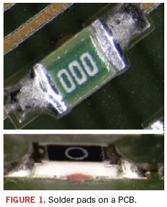
Pad it. Pad dimensions should be carefully considered on the bottom-side SMT of a double-sided mixed board. This includes extra thieving pads for wave-soldered ICs and extended toe pads to facilitate solder wicking. Both can significantly improve the yield at wave soldering (Figure 1).
In addition, components on the board should be oriented so that the solder joints are not shadowed as the board moves through the wave solder.
Clear it. If a double-sided mixed board is so dense that the above guidelines cannot be observed, a special fixture called a selective wave fixture (also known as a pallet) into which the board is snapped can be used. This masks the bottom-side surface mount from exposure to the wave. To do this, there must be sufficient clearance (0.1") between the PTH and SMT lands on the solder side so that the SMT can be masked by the fixture (Figure 2).
Keep in mind that fixtures add cost to the product; several fixtures are required, at several hundreds of dollars per fixture, and they have to be cleaned, loaded, unloaded and occasionally replaced.
Think single-sided. Overall, when designing a mixed board (using SMT and PTH), it pays to think single-sided! If possible, PTH parts should be placed on the same side of the board as the primary SMT devices. Double-sided PTH or PTH on the wrong side is almost certain to require manual soldering. There is just no other way to process them cost-effectively with existing automation.
George Henning is vice president of manufacturing at OCM Manufacturing (ocmmanufacturing.com); This email address is being protected from spambots. You need JavaScript enabled to view it..