What are bottom termination components? You may not know the term “BTC,” but because IPC is focusing on these packages, expect to hear more about them.
IPC has coined the term BTCs for descriptive package names such as QFN, DFN, SON, LGA, MLP, etc. They are in some ways similar to BGAs, which also have hidden terminations, but they are also very different. They do not have balls, but rather, metalized terminations or pads underneath the package.
“PCB Design and Assembly for Flip-Chip and Die Size CSP” Author: Vern Solberg; This email address is being protected from spambots. You need JavaScript enabled to view it.. Abstract: This paper outlines the basic elements furnished in the newly released IPC-7094, Design and Assembly Process Implementation for Flip-Chip and Die Size Components, providing a comparison of existing and emerging wafer-level and chip-size package methodologies. The focus is on the effect of PCB design and assembly of bare die or die-size components in an uncased or minimally cased format. (IPC Apex, April 2010)
Solder Joint Defects
“Telecommunications Case Studies Address Head-in-Pillow (HnP) Defects and Mitigation through Assembly Process Modifications and Control” Authors: Russell Nowland, Richard Coyle, Peter Read and George Wenger; russell.nowland@ alcatel-lucent.com. Abstract: This paper discusses several contributing factors to the head-in-pillow defects and techniques to control them. The case studies presented show that process control can mitigate HnP defects, but may not be successful for some severe examples of HnP defects. The case studies include reviewing paste printing modifications, solder paste DoE, shadow moiré scans on several problematic BGA packages, effectiveness of x-ray inspection, and cross-section analysis of failed HnP solder joints. Together, these case studies show that BGA package warpage is a major contributor, but HnP defects can occur when almost any of the assembly process parameters deviate from acceptable practices. (IPC Apex, April 2010)
Solder Joint Inspection
“Robust Automated Void Detection in Solder Balls and Joints” Authors: Asaad F. Said, Bonnie L. Bennett, Lina J. Karam and Jeff Pettinato; This email address is being protected from spambots. You need JavaScript enabled to view it.. Abstract: This paper proposes a robust, accurate, and automatic void detection algorithm. The proposed method is able to detect voids with different sizes inside the solder balls, including the ones that are occluded by board components and under different brightness conditions. The proposed method consists of segmenting individual balls, extracting occluded balls, and segmenting voids inside the solder balls. Segmentation of the individual balls is achieved by using the proposed histogram and morphological-based segmentation method. (IPC Apex, April 2010)
In the RoHS world, sharing supply lines has forced a change on defense contractors.
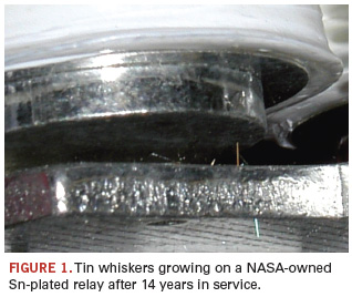
While electroplated SnPb surface finish exhibits good solderability and is virtually immune to tin whisker growth, a termination plated with pure tin is very likely to spawn tin whiskers, usually in months or years after plating (Figure 1). Tin whiskers, being electrically conductive, have been the cause of short-circuit failures.
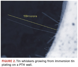
RoHS has similarly compelled board fabricators to final finish solder pads with electroless nickel/immersion gold (ENIG), immersion tin, or immersion silver (since all are Pb-free) instead of the SnPb hot air solder level (HASL) finish used successfully for some 60 years. Immersion tin has shown a propensity to permit tin whisker growth (Figure 2). Immersion silver reacts with sulfur-bearing atmospheres to form nonconductive silver sulfate, which then reacts with any exposed copper on the board to form nonconductive copper sulfate, which also causes board failure. The long-used ENIG finish is still usable under RoHS, with no major drawbacks.
When selecting components and circuit boards, the military, in spite of being exempt from RoHS, uses the same supply lines as non-exempt commercial electronics firms. It comprises too small an annual volume to influence the market (e.g., surface finish) for components or boards.
The military would prefer to have all component terminations (and PWBs) finished with the known reliable SnPb alloy rather than pure Sn, because the lead content in the tin prevents the potential of tin whisker-induced failures in electronics systems (Figure 3). To overcome the whisker risk with pure tin-plated (albeit RoHS-compliant) components (the only ones available), critical military electronics require expensive and time-consuming refinishing of component terminals. This usually is done by dipping the tin-coated component contacts in molten SnPb solder, one at a time.
Because of RoHS, the military is forced to accommodate the added expense and time of refinishing electronics component terminations. Adding to that turmoil, component refinishing adds the risk of thermally damaging the dipped components due to the hot-dipping procedure, potentially reducing the reliability of Pb-free electronics.
The US Department of Defense now is challenged to develop a department-wide policy that will preserve the reliability of SnPb electronics. This policy will inevitably include the idea of a Lead-Free Control Plan (LFCP), documenting methods used by each DoD supplier to mitigate risks for every item of electronic hardware acquired by any DoD program. This acquisition policy would cover any electronics, commercial off-the-shelf (COTS) or otherwise, for any military use. One uniform policy across all DoD components (services and agencies) would go a long way toward mitigating confusion among vendors about the need and techniques to limit Pb-free electronics risks.
ACI Technologies Inc. (www.aciusa.org) is the National Center of Excellence in Electronics Manufacturing, specializing in manufacturing services, IPC standards and manufacturing training, failure analysis and other analytical services. This column appears monthly.
Continuous improvement relies on a balance between well-defined strategy and effective execution.
Pick up any industry trade magazine or attend any conference and you invariably are exposed to the current slate of “hot topics”: Consolidation. Merger. Acquisition. Vertical integration. NADCAP, AS9100, ISO 13485 certification. New materials, new processes, new equipment. Reliability and quality. Low-cost geography. Quick turn. Intellectual property.
All are valid and valuable strategic elements. Yet, it has been said that vision – or in this case, strategy – without action is nothing more than dreams. But when you thoughtfully merge vision and action, the result is real, meaningful progress. So in today’s wild and changing environment, how do we turn these important strategic initiatives into world-class progress by effectively merging this vision and urgent action? What is the execution plan?
This author believes there are three key components to this vision/action merger: the growth of an effective Lean Six Sigma methodology forming the foundation of a culture of continuous improvement, the embrace of a vital and vibrant employee development program, and the presence of an effective leadership structure and system.
The various Lean methods and Six Sigma problem-solving techniques have been well documented, and need not be discussed here in great detail. But to any degreed engineer, a large part of the Six Sigma toolkit is what was originally taught to us as “The Scientific Method.” The Scientific Method was the cornerstone of every science class in high school and college. So, if these methods are so common and so well known, what’s the big deal? It is that the methods are not followed due to a fundamental lack of problem-solving discipline and the quest to put out the latest fire. Often, these fires are only superficially solved, left smoldering, waiting to flare again, since the true root cause was never identified and subsequently extinguished. Human nature is to deal with what will get you shot today, and a problem that went away will not get you shot (at least not today). That being the case, the Six Sigma structure and methodology is genuinely valuable because it drives a set of problem-solving methods and disciplines that value true root cause analysis, and thus prevents problem recurrence. These tools and techniques foster a data-based decision-making culture via broad use of statistical process control, well designed experiments, automated statistical analysis tools, and the use of Ishikawa fishbone diagrams and the “Five Why’s” for root cause analysis. Once a problem is solved, the proper controls are put in place, and that specific problem should never happen again. You never want to buy the same real estate twice.
Lean methodology is also critical, especially in manufacturing settings where a constantly changing product mix will quickly obsolete run rules aimed at maximizing efficiency. The variable product mix issues are amplified by new product introduction and their aggressive schedules. As such, setup reduction and lot size optimization are constant challenges and critically important, perfect applications of the Lean tools, including manufacturing associate-driven kaizen events. Lean methods, including 5S and work cell standardization, will always help improve factory efficiency, optimize overall throughput, and set the stage for effective Six Sigma tool use.
One of the beneficial improvements driven by Lean implementation is cycle time reduction. Cycle time reduction obviously is desirable to customers; shorter lead times are regularly used as a competitive tool in the sales force arsenal. But the operations team loves cycle time reduction too. A shorter build cycle time means more cycles of learning available per quarter, which accelerate iterative yield learning. Similarly, in the event of the unavoidable process problem, shorter cycle times reduce mean time to detection, and minimize the amount of work in process that may be affected. (Of course, reduced cycle times also are attractive to the CFO, for cash preservation reasons.)
Many of these initiatives start with a flourish, but then settle into a business-as-usual approach, especially if the initiative is treated as a program, rather than a new way of life. To cement these tools in the organization, one needs a comprehensive training system to proliferate these tools, with a situational delivery method to accommodate different incoming skill levels. A haphazard education system that results in a cultural backslide will be exceptionally discouraging to those who enthusiastically volunteered a few short months ago. Manufacturing teammates want to do a better job and want to be more involved, and if education and problem-solving participation is dangled in front of them without a sustainable system for 100% inclusion, the result will be far worse than before the start of the initiative. I’ll reiterate: this is not a program, but a process aimed at sustainable, continuous improvement. The employee development program cannot simply offer single-ended Lean or Six Sigma training. A truly effective program will address a wide variety of topics within the three skill sets: job content skills, transferable skills and self-management skills. All three must be collectively addressed with the individual’s personal readiness taken into account, and the resultant training must be immediately put to use on the production floor so that the skills are not merely theoretical in nature, but have been reduced to practice in a meaningful way. Employee development is a long-term investment too often sacrificed during tough financial times. This is a mistake.
Strong, vibrant leadership is the last key component, the glue that holds all this together, as well as a catalyst to make the organization more effective. Great leaders show their mettle under fire. There is a marked difference between leading and managing. Managers, by definition, manage, or react to situations after they arise. In stark contrast, leaders exercise a more predictive, anticipatory approach to their responsibilities, which always has the team moving forward in sync with the overall organizational strategy. All too often, people are put into leadership positions because they had historically been a great doer, a great problem-solver. But are they a great problem avoider? The leader is truly a catalyst, employing an effective organizational structure that fosters timely, penalty-free communication and has interlocked and cascaded SMART goals: specific, measurable, attainable, realistic and timely. Since people respect what you inspect, these goals link directly to a handful of bellwether metrics, from which the pulse of the operation can always be taken.
Many strategies can be incorporated into an organization’s operating plan. Execution and the tools to enable execution are the missing link. The proper balance between a well-defined strategy and an effective execution plan will form the foundation for a culture of continuous improvement. One without the other is counterproductive. Once this culture takes root, however, and the entire organization’s efforts are synchronized and catalyzed, the result is unstoppable.
James Fuller is vice president, development at Endicott Interconnect Technologies (eitny.com); This email address is being protected from spambots. You need JavaScript enabled to view it..
No industry trends stayed secret at ECTC in Las Vegas.
In early June, almost 900 people gathered in Las Vegas at the Electronic Components and Technology Conference – not necessarily to seek fortunes in the casinos, but to roll the dice on the next big trend in the electronics industry. Bet correctly on the right packaging and assembly trend, and revenues will multiply; bet wrong by installing capacity for a technology not in strong demand, and you could lose it all. Given ASE COO Dr. Tien Wu’s prediction of less than double-digit growth on the semiconductor side, the backend packaging and assembly projects to where the action will be.
Get med. The World Health Organization predicts that by 2025 more than 1.2 billion people will be over 60 years old. Given such projections for an aging population, medical electronics has tremendous growth potential. In the field of imaging, the US market is somewhat saturated for equipment providing CT scans, ultrasounds, x-rays and MRI, but portable medical devices such as defibrillators and portable ultrasounds are experiencing strong growth. Increased demand for implantable devices is anticipated for infusions, pumps, pacemakers, and even drug delivery systems. For these systems, miniaturization is key, and lessons from today’s handhelds segment may be applicable. One critical difference is that, when one drops a cellphone and it stops working, one might be unhappy, but if a pacemaker stops working, the user could be dead. Here, reliability cannot be understated. With many components only available with Pb-free finishes, companies must determine what strategy will be best to mitigate any issues. Greater use of conformal coatings, underfill materials, and encapsulants is anticipated.
Mobile architectures. The convergence of computing and communication is clearly seen in the mobile devices of today and tomorrow. Key themes discussed in this year’s ECTC plenary session focused on mobile processing architectures. The demand for increased mobility, multimedia functions, connectivity, and bandwidth is driving new technology and infrastructure developments. Companies such as RIM are increasingly focused on incorporating in smartphones’ new features such as multimedia, navigation, games, social networking, and productivity enhancements. While many of today’s smartphones use package-on-package (PoP), roadmaps include the possibility of 3D through silicon via for memory and processors. Cost remains a major focus in the adoption of any new package architectures. The introduction of Apple’s iPad calls into question how future products will be designed – starting not with the semiconductor and board layout, but instead with the user interface, screen, touch pad, and battery life.
Bright lights. With government mandates for the switch to LED lighting, the market for high brightness LEDs is expected to grow. Packaging and assembly of high brightness LEDs is increasingly recognized as critical in reducing product cost and enabling reliability. Packaging has to satisfy requirements for form, fit and function, but must also provide a conductive thermal path for the heat and meet requirements for optics. Improper heat dissipation can degrade materials and impact the performance of the luminaries. Lighting applications will provide an exciting area as engineers solve challenges with material interactions.
3D TSV. The industry clearly has moved from “PowerPoint engineering” to the hard work and challenges of materials science and real engineering in 3D through silicon via. More than 50 of the approximately 323 papers at ECTC discussed 3D TSV, with most discussing process improvements. Over the next year, companies and research institutes will be saying less and doing more to resolve manufacturing issues and challenges associated with moving from R&D projects into commercialization. Improving yield is critical to meeting cost-reduction goals. Reliability data should be forthcoming if development targets are met.
Assembly trends. With the price of gold hovering around $1,200 per oz., many companies are riding the wave of copper wire bonding. While there are still technical challenges, much progress is being made and cost is the driver. Examining the cost tradeoffs with each technology is becoming increasingly important. An increasing number of devices are transitioning from wire bond to flip chip. Companies are looking at finer pitch bumps and Pb-free solutions that will work with new ultra low-k dielectric materials used on the device. Many companies are interested in copper pillar as a means to reduce cost. According to STATS ChipPAC, the use of molded underfills for flip chip in strip format and designs to reduce substrate complexity have gained attention in the past year.
Wafer-level packaging remains an exciting topic, and many ECTC papers examined improved reliability for mobile applications. Small diameter balls are in production, and pitches as fine as 0.3 mm are gaining acceptance. Fan-out WLPs are shipping in volume production for high I/O parts. Capacity expansions are underway and new developments are expected as the technology is extended to stacking.
The remainder of the year promises to be exciting for the backend assembly and packaging companies. Equipment and materials sales are improving and new challenges call for closer cooperation between suppliers and users.
E. Jan Vardaman is president of TechSearch International (techsearchinc.com); This email address is being protected from spambots. You need JavaScript enabled to view it.. Her column appears bimonthly.
The new “package of the day” requires modified paste layers.
Modules with castellated mounting holes are showing up more and more these days. I’ve also heard it called a “half-via” setup. Both seem to fit. The copper mounting pads on the bottom of the module’s little PCB wrap up the side of the PCB with a half-via. Thus the name “half-via.” If looked at from the base, the edge does look a bit like the outline of the top of a castle wall, so that makes sense too.
Whatever. The name isn’t that important. A few things are important though, such as the land pattern and solder deposition. I hadn’t heard any special requirements for using this type of part until recently, when I ran across a GPS receiver module from ublox (u-blox.com). What they say is that more solder is needed on the outside of the pad than on the underside of the pad, so it can properly wet up the half-via. That makes perfect sense. There are probably multiple ways of doing this, but you can see their take on it in their data sheet (Figure 1).
Obviously, follow the data sheet that comes with your specific part, but if you don’t have any official guidance and can’t get word from your part manufacturer’s applications engineers, this method might provide a hint. The copper land is just a standard rectangle, as is the solder mask. The paste layer, however, is not. It’s wider toward the outside of the part. This will help create a proper fillet up the via, while reducing the chance of solder balls and other messy things that can happen when you have too much solder under a part.
All that said, when did this become the package of the day? I haven’t seen what IPC has to say about it yet, but these things are all over the place. Our engineers and assembly folks are cool with it. It’s not that tough to build, fortunately. But, as I saw with the u-blox GPS part, there are new design issues to contend with. I can certainly see the advantages of the package. The half via can permit a good solid fillet, providing good mechanical connection. They’re typically a PCB-type substrate, so the coefficient of expansion and flex strengths should be similar to the underlying PCB. On the other hand, like with an LGA (land grid array), the low profile after soldering will tend to exacerbate an expansion or flex risks.
If you happen to be in the business of creating modules that use this form factor, you can do a few things to help designers and manufacturers out. First, and most important, make sure to put a good pickup place centered on the topside of the module. It can be a metal EMI shield or a big part with a nice flat surface. Either should work, but without that pickup point, most manufacturers will end up hand placing it and that doesn’t bode well for high-volume use of the part. On the bottom, put a decent sized pad along with the half-via. I’ve seen some that just use the via’s annular ring. Don’t do that. It doesn’t give enough room for a good solder joint.
Duane Benson is marketing manager at Screaming Circuits (screamingcircuits.com); This email address is being protected from spambots. You need JavaScript enabled to view it.. His column appears bimonthly.