The electronics manufacturing industry will remember 2010 for many reasons: rampant component shortages (and the rise of counterfeits), the tight financial markets and tense end-market conditions.
But mostly, it will remember 2010 for the long-awaited recovery.
EMS shook off the doldrums of 2008-09, demonstrating tremendous resilience and yes, patience, as demand easily outstripped supply throughout the calendar year. It also showed it remembered the lessons from 1999 to 2001, where unprecedented OEM demand led to acquisition sprees and six-month order lead times. It took two years for that hangover to end.
Not this time.
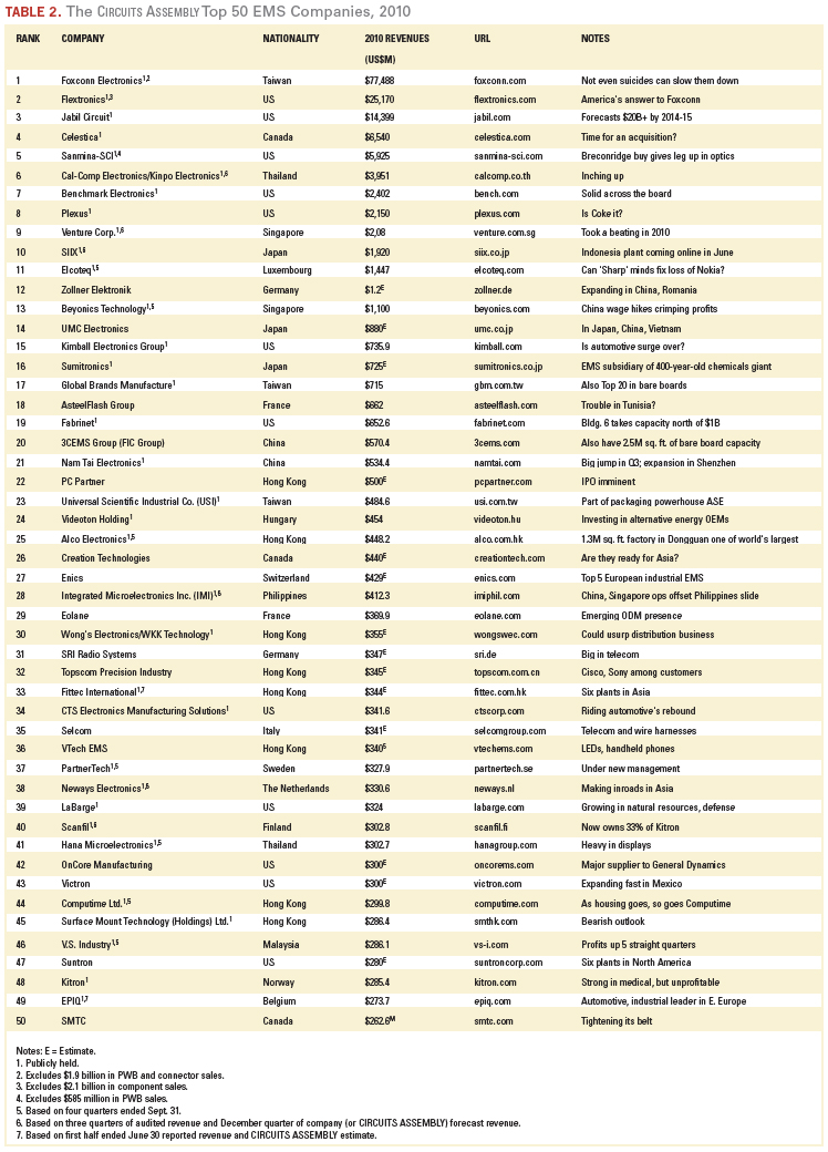
Expansion occurred, of course, but it was targeted. Even Foxconn, which announced or opened several sites in China during 2010, didn’t bring on capacity so much as it relocated it inland from the Shenzhen area, where inflation and negative attention coupled with a parade of worker deaths made the “Walled City” environs even more uncomfortable than usual. Most followed the lead of companies like Zollner, which expanded two plants in China, but left the rest of its footprint as is. Acquisition activity was also held in relative check. The big deal of the year was Sanmina-SCI’s purchase of Breconridge (No. 48 in last year’s revised Top 50). Smaller deals abounded, but were generally on the order of the MC Assembly’s pickup of Chase Corp.’s EMS operations or ElectronicNetwork’s snatching of Görmiller from bankruptcy, tidy deals that were quickly accretive and added 10 to 15% in revenue to the balance sheet but didn’t do much insofar as moving the needle on the CIRCUITS ASSEMBLY Top 50 chart.
Falling off the Circuits Assembly Top 50 this year was Hitachi Computer Products, as expected, as the Oklahoma site ceased taking outside orders to concentrate on its parent company’s production needs. Jumping in were a handful of firms that were unintentionally omitted in 2010. They include Japan’s UMC Electronics and Hong Kong’s PC Partner, Topscom and Fittec.
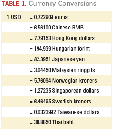
Currency fluctuations did not have a profound effect on this year’s results, as most of the major currencies were fairly stable with last year, trading in a band of 3 to 5 percentage points. The exception was the Japanese yen, which had fallen 9.5 points against the dollar from Feb. 1, 2010 to Feb. 1, 2011, the date used for the conversions (Table 1).
While the big clearly got bigger, the middle class acquitted itself nicely (Table 2). No. 30 Eolane finished 2010 with 268 million euros in revenue, up 72% from 156 million euros last year. No. 19 Fabrinet (the early leader for 2011’s CIRCUITS ASSEMBLY EMS Company of the Year) shot up 72% as well on demand for optical networks. No. 38 Neways was up 27%. In North America, military/industrial suppliers On Core and Victron each grew around 20%.
[Ed.: To enlarge the table, right-click on it, then click View Image, then left-click on the table.)
There was little change among the top 10 companies from 2009. Foxconn remains the clear-cut leader, well ahead of No. 2 Flextronics, which lost ground despite growing its EMS sales by $3.5 billion last year. No. 3 Jabil (up 23%) extended its lead over the rest of the pack, and management has plans to top $20 billion within four years. No. 5 Sanmina’s aforementioned acquisition of Breconridge helped it close the gap with No. 4 Celestica. Benchmark rose two spots to seventh and No. 10 Siix leveraged a huge year (up more than 35%) to displace Elcoteq, last year’s No. 7, from the Top 10. Venture, last year’s No. 8, slipped one spot.
The 2009 recession lowered the bar for entry into the Top 50. The cutoff for last year’s revised list was almost $200 million. 2010 changed that. For this year’s list, the cutoff was about $263 million, leaving worthy companies such as KeyTronic EMS out of the chart.
Still, the rising tide did not lift all regions, let alone all ships. While North American and Asia generally rebounded, the EMS industry in Europe continued to list. Kitron, Scandinavia’s third-largest EMS after Elcoteq (which is based in Luxembourg in name only) and PartnerTech, suffered through component shortages, plant closures and management changes. After eight straight quarters of losses, No. 11 Elcoteq turned profitable in the first quarter of 2010, and in the June period broke a streak of six consecutive quarters of falling revenue. Still, the third quarter saw lower sales and more losses, leaving the company-estimated sales down 30% for the year; the firm dropped out of the Top 10. On the other side of Eurasia, Hong Kong’s Alco’s revenue slid 33% from last year, and its ranking fell likewise (to No. 24 from No. 16).
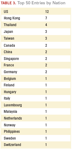
By country, the US remains the home to the largest share of the biggest players (Table 3), with 12 entries, one less than in 2009. Hong Kong rose by two, to seven, the result of two omissions from last year’s Top 50. Canada lost an entry to an acquisition. The UK, once home to powers like MSL, was left without a single entry.
Of course, for many companies, the “home nation” is more a formality than a reality. For Foxconn, Flextronics, Beyonics, GBM, and several others, China is their largest footprint. Fabrinet is headquartered in San Francisco, but the vast majority of its factories are in Thailand. Given the violent uproars in the Middle East and much of Africa, it is safe to say there won’t be any new EMS facilities in those regions soon. As such, Table 3 will likely be very similar next year as well.
CIRCUITS ASSEMBLY is not the only entity that tracks the top EMS players. So why does our list occasionally disagree with those of other industry watchers? One reason is that we make our best effort to count only the revenues derived from EMS sales. Thus, companies like Foxconn, Flextronics, Hana Microelectronics, OSE, Sumitronics and Sanmina-SCI appear tens of millions and sometimes billions of dollars smaller than they truly are. Our belief is this gives a truer picture of the actual EMS sales, as opposed to revenue from connectors, bare boards, sensors or other unrelated components.
A few words about Foxconn. Although it is undisputedly the world’s largest ODM/EMS player, Foxconn is almost inscrutable. Most industry watchers know it is a major supplier to Dell, H-P, Sony and, of course, Apple, but plenty of smaller OEMs use its services too. Besides EMS, it is one of the world’s largest bare board fabricators – sales reportedly are somewhere between $700 million and $1 billion – and is among the top 10 in connectors too.1 It is quickly becoming a major supplier of LCD screens (which suggests Apple TV is not far off), and is headed toward a top 3 position in branded motherboards. Some rumors about the company are occasionally so off-the-charts outlandish, such as one making the rounds last fall suggesting Foxconn would invest $10 billion (not a typo) in a plant in Chengdu, China, that it’s a wonder how they get published.
But there’s the rub. Though public, Foxconn is traded on the Taiwan Stock Exchange, whose standards are relaxed relative to other major exchanges, and accordingly, the company-reported data are incredibly vague. What would seem its primary website, foxconn.com, hasn’t been updated in months. Its subsidiaries, such as cellphone ODM unit Foxconn International Holdings, sometimes have related names, but other times they don’t (witness Q-Run and Hongfujin Precision Industry Co.). And its subsidiaries have subsidiaries: Hongfujin reportedly is China’s largest exporter and has at least 60 other companies under it, which combine for roughly $30 billion in revenue.2 It has begun to open retail stores in China under the name Cybermart; it’s unclear how much revenue the 35 or so sites have generated thus far, but given Foxconn’s size, it’s unlikely to be material. Is Foxconn as large as the figures claim? It says here, no. But very few people can know for sure.
References
1. Ron Bishop, “The Top 10 Connector Companies,” ConnectorSupplier.com, August 2010. 2. Ling Ruiming, “Foxconn Faces Tough Competition from Rivals,” China Daily, Nov. 30, 2009.
Mike Buetow is editor in chief of Circuits Assembly; This email address is being protected from spambots. You need JavaScript enabled to view it..
Ed.: Due to a currency translation error, Team Precision is incorrectly listed in the Top 50. Team Precision's actual calendar 2010 revenue was about $71.3 million. SMTC, at $262.6 million, should have been ranked 50th. Also, due to a spreadsheet miscalculation, VTech EMS' revenue was initially incorrectly calculated. We regret the errors.
Problems related to conductive pastes as fillers have led to the development of electrolytes.
To etch fine conductive patterns (75 µm lines/spaces) of the panel plated copper without excessive underetching, the total copper thickness (Figure 1) before etching must be correspondingly low. While copper thickness can be reduced by performing one or more copper thinning cycles, as shown in Figure 2, this increases costs and reduces productivity.
Productivity can be increased and costs reduced by eliminating the copper thinning step or, at least, reducing the number of copper thinning cycles. To permit this, the total thickness of the copper layer (Cu laminate + Cu strike layer, if present + Cu blind microvia filling) on the PCB must be reduced. A number of PCB manufacturers therefore specify a maximum copper layer thickness of 25 µm. This means that only approximately 18 µm of copper may be deposited on the PCB surface during the blind microvia filling process step. Besides the advantages in terms of productivity and costs, this also implies less waste of material because less copper has to be plated and etched subsequently.
Processes for blind microvia filling by copper electroplating have been used in volume for a number of years, principally in Asia. To achieve the required coating properties, these processes use high-leveling sulphuric acid copper electrolytes containing organic bath additives alongside copper sulphate, sulphuric acid and chloride. Several types of blind microvia filling electrolytes are now commercially available from a number of suppliers. The various processes differ in the following areas:
Organic additive system.
Anode material (copper anodes or insoluble anodes).
Applied current form (direct current or reverse pulse plating).
Type of plating line used (standard vertical, vertical
continuous or horizontal continuous).
Applicable current density.
A typical filling result achieved with current generation electrolytes results in a plated copper thickness of 22.7 µm, exceeding the limit of 18 µm required for 75 µm/75 µm lines and spaces. To meet this limit, new electrolytes offering improved filling performance needed to be developed. The objective is to deposit less copper onto the surface of the PCB than previously, while achieving at least comparable filling. This is often referred to as “superfilling.” In addition, plating times must not be longer than in established processes, and continued use of present plating equipment should be possible.
Figure 3 shows the filling achieved with this new electrolyte in a blind microvia with dimensions of 100 µm θ and 65 µm depth. Copper thickness was reduced from 22.7 µm to 10.7 µm for a plating time of 60 min. at a current density of 1.5 A/dm2. The dent is 7.6 µm.
The novel electrolyte significantly reduces copper thickness, while also achieving a slightly better filling. (The dent is shallower.) The plating time was shortened by 8 min. In addition, the novel electrolyte can be used in the same plating plant as its predecessor and does not require any alterations to equipment.
The performance of the novel electrolyte will first be demonstrated for the requirements dent < 10 µm and copper thickness < 18 µm. PCBs (size: 500 mm x 400 mm) with blind microvias (Ø: 100 µm, depth: 80 µm) were copper-plated in a 1400-litre test module equipped with insoluble anodes. This test module is identical in construction to the electroplating module of a vertical continuous plating line introduced into market a few years ago. Unless otherwise stated, all tests were carried out using PCBs that were treated with electroless copper.
Figure 4 shows the filling achieved after plating for 75 minutes at 1.2 A/dm2. The blind microvia is completely filled with copper; the copper thickness is 15.8 µm, and the dent is 0 µm.
The filling achieved with these parameters is excellent, but at a current density of 1.2 A/dm2, productivity is insufficient. Completion of blind microvia filling within a maximum of 70 min. was therefore requested. In the subsequent test, plating time was reduced from 75 to 60 min., and current density increased from 1.2 to 1.5 A/dm2, so the same amount of electric charge was available for copper-plating in both tests. Figure 5 shows that complete blind microvia filling was achieved, even with a shorter plating time of 60 min. The dent increased from 0 µm to 9.5 µm, while the copper thickness remained practically unchanged. This result shows the new process is able to fulfill the requirements regarding dent and copper thickness outlined above.
Figure 6 shows the filling result achieved when a copper strike was applied. With a copper strike, the dent is reduced from 9.5 µm to 6.3 µm.
The pre-reinforcement of the conductive layer (electroless copper or direct metallization) with an electroplated copper strike is an ideal base layer for subsequent filling. A thin copper layer with a thickness of only 2 to 5 µm is sufficient. Appropriate pre-treatment (e.g., acid cleaner) produces an active copper surface that facilitates a very quick onset of the blind microvia filling. With all other parameters unchanged, this results in an improved filling. Application of a copper strike frequently permits blind microvia filling to be carried out at higher current densities, leading to shorter plating times. In the tests described herein, the copper strike was produced using an electrolyte used for copper plating blind microvias in volume PCB production.
If lower requirements for blind microvia filling (e.g. dent < 25 µm) and copper thickness (e.g. copper thickness < 25 µm) are possible, very good results can be achieved with the new electrolyte, even with short plating times and high current densities. For blind microvias (Ø: 100 µm, depth: 80 µm) a dent of 13.3 µm, a copper thickness of 22.3 µm is achieved with a current density of 2.0 A/dm2 and a 55-min. plating time (Figure 7a). Increasing the current density further to 2.5 A/dm2 produces a dent of 20.9 µm and a copper thickness of 23.3 µm over a plating time of only 45 min. (Figure 7b).
The new electrolyte can also produce a good filling in large size blind microvias. These have a larger volume, meaning more copper is required for filling, and the plating time for a current density of 1.5 A/dm2 needed to be prolonged to 90 min. For a blind microvia (Ø: 100 µm, depth: 100 µm), a dent of 4.4 µm and a copper thickness of 24.6 µm was achieved (Figure 8a). For a significantly larger blind microvia (Ø: 150 µm, depth: 100 µm), a dent of 20.2 µm and a copper thickness of 23.7 µm could be achieved (Figure 8b) using the plating parameters as mentioned above.
Direct metallization. The new blind microvia filling electrolyte can also be used for PCBs that have been treated with direct metallization. Figure 9 shows the filling achieved on a PCB treated using a graphite-based direct metallization process. However, with unchanged plating parameters, slightly worse filling was achieved compared to the PCB treated with electroless copper (Figure 5).
Copper strike deposition improves blind microvia filling considerably, even on PCBs treated with direct metallization. Figure 10a shows a blind microvia (Ø: 110 µm, depth: 60 µm) in a PCB treated with graphite-based direct metallization after deposition of a copper strike. It is clearly apparent that the copper strike was not deposited conformally, and that the copper thickness is greater in the area of the capture pad/dielectric transition. In combination with the active surface of the copper strike, this geometry provides ideal conditions for subsequent blind microvia filling and permits a higher current density and shorter plating time to be used. Figure 10b shows very good blind microvia filling after deposition at 1.9 A/dm2 over 50 min.
Pattern plating. The novel electrolyte can also be used for pattern plating (Figure 11), but few experimental data are currently available.
Through-hole plating. The novel electrolyte can also be used for plating through-holes (Figure 12). However, it should be noted that good throwing power between 70 and 100% can only be achieved with thin PCBs and low aspect ratios. As with pattern plating, few experimental data are currently available. Alongside electrolyte and plating parameters, the blind microvia filling result is also strongly dependent on the size and shape of the unfilled blind microvias. The best filling results are achieved with conical blind microvia shapes. However, blind microvia shapes encountered in practice often deviate significantly from this ideal. Depending on the dielectric type and the laser drilling parameters, recessions can result (see circles in Figure 13aand b).
The new electrolyte for blind microvia filling also permits overhangs and recessions to be filled with copper without defects (see circles in Figure 14). A copper strike was used in this case.
Reliability. The reliability of electroplated copper layers is an important quality criterion in PCB production, and appropriate reliability tests must be performed on an ongoing basis. The copper layers deposited using the novel electrolyte exhibit an elongation of about 20% and pass the reliability tests in Table 1.
The electrolyte is made up with copper sulphate, sulphuric acid and hydrochloric acid, and contains three organic bath additives alongside the inorganic ingredients. The concentration ranges of each of the electrolyte components are in Table 2. To ensure a good blind microvia filling, it is quite common that the copper ion concentration in blind microvia filling electrolytes is significantly higher in comparison to other copper electrolytes for PCB production.
The methods used for analysis of the individual electrolyte components are summarized in Table 3. The leveler content of the electrolyte can be evaluated by plating a Hull cell panel. A cyclic pulse voltammetric stripping (CPVS) method for leveler analysis is currently under investigation.
Operating conditions. The main operating conditions for the new electrolyte are shown in Table 4. The electrolyte is used under direct current conditions and with insoluble anodes at a maximum temperature of 22°C. Replenishment of copper ions is performed by dissolution of copper oxide in a separate dissolving unit and subsequent addition to the plating tank. It is preferable to operate the electrolyte in a vertical continuous plating (VCP) line. This equipment combines the advantages of horizontal continuous plating lines with those of standard vertical plating lines. The electrolyte may also be used in standard vertical plating equipment, but VCP lines generally produce somewhat better results.
The novel electrolyte for blind microvia filling has been used in a VCP line in mass production of PCBs (line/space 75 µm/75 µm respectively 60 µm/60 µm) for about nine months. Filling of blind microvias (Ø: 110 µm, depth: 60 µm) is carried out at a current density of 1.5 A/dm2 over a plating time of 52 min. The dent is less than 10 µm. The resultant copper thickness is approximately 15 µm, and this can be reduced to the final thickness required for the subsequent tent and etch process by a single copper thinning cycle.
Before the new electrolyte was available, its predecessor was operated in the same plant. Using this previous electrolyte, complete blind microvia filling was achieved with the same current density of 1.5 A/dm2, but a plating time of 68 min. However, the copper thickness achieved was approximately 20 µm, requiring the copper thinning process to be repeated multiple times.
Thus the new electrolyte permits both the blind microvia filling process and copper thinning process to be carried out more quickly.
Summary
The superior filling performance of the new electrolyte permits blind microvias (Ø: 100 µm, depth: 80 µm) to be completely filled with electroplated copper (dent < 10 µm), while producing a lower copper thickness (< 18 µm) on the PCB surface. This enables blind microvia filling and line/space 75 µm/75 µm respectively 60 µm/60 µm via tent and etch process without requiring multiple copper thinning cycles. This increases productivity, reduces costs and leads to less waste of copper. In case of lower dent and copper thickness requirements, blind microvias (Ø: 100 µm, depth: 80 µm) can be completely filled with copper over even very short plating times. Even very large blind microvias (Ø: 150 µm, depth: 100 µm) can be completely filled with copper over reasonable plating times.
The new process can also produce HDI PCBs treated with graphite-based direct metallization processes. A copper strike can be applied to increase the filling further, both with direct metallization and with electroless copper.
The electroplated copper layers meet the common reliability test requirements for PCBs.
Experience with the electrolyte in mass production of HDI PCBs to date shows that the new electrolyte permits stable and reliable blind microvia filling.
The electrolyte can also be used for pattern plating and through-hole plating, but only a small amount of experimental data is currently available.
Acknowledgments
The author would like to acknowledge the support of AGES Group (Taiwan), and particularly Albert Yeh, in this project.
Bibliography
1. T. Teng, “iSuppli Issues Fast Facts on Latest iPhones,” June 7, 2010. 2. J.W. Stafford, “Semiconductor Packaging Technology,” Printed Circuits Handbook, 5th edition, McGraw-Hill, 2001, pp. 2.1 - 2.22. 3. C.F. Coombs and H.T. Holden, “Electronic Packaging and High-Density Interconnectivity,” Printed Circuits Handbook, 5th edition, McGraw-Hill, 2001, pp. 1.3 - 1.22. 4. M. Carano, “Electrodeposition and Solderable Finishes for HDI,” The HDI Handbook, 1st edition, ed. by H. Holden, BR Publishing, 2009, pp. 355 - 397. 5. H. Holden, “The HDI Manufacturing Processes,” The HDI Handbook, 1st edition, ed. by H. Holden, BR Publishing, 2009, pp. 231 - 257.
Ed.: This article is adapted from a presentation at SMTA International, October 2010, and is published with permission of the author.
Michael Dietterle, Ph.D. is with Max Schlötter GmbH (schloetter.de); This email address is being protected from spambots. You need JavaScript enabled to view it..
Differences in maximum ripple current and ESR can lead to a shift in the ripple current – and premature failure.
During the design of a power supply, careful consideration must be given to the equivalent series resistance and ripple current, as well as the total output capacitance. The capacitors should be as identical as possible, with the same ESR and ripple current capacity.
Early life failures can occur as a result of using two different capacitors. In the case below, the capacitance value and working voltage rating of each were the same. However, the maximum ripple current and ESR were substantially different. This causes a shift in the ripple current through the capacitors and caused the supply to fail prematurely.
The design of the power supply called for the following:
Maximum ripple current: 1400mA.
Maximum allowable ESR: 50mΩ.
Total capacitance: 940µF.
This design used two different capacitors in parallel to meet these requirements. One capacitor was a Series A capacitor, while the second parallel capacitor was a Series B capacitor. Table 1 compares the two capacitors. The capacitors were well matched, except in two areas: the maximum allowable ripple current and the ESR.
The ESR of a capacitor acts as a resistance in series with the capacitance (Figure 1). The difference in ESR meant that the ripple current did not split evenly between the two capacitors. Equation 1 shows the calculation of current through the resistors (and hence the capacitors).
Given the values shown above and the estimated total ripple current of 1400mA, IR1 is ~500mA (640mA max), while IR2 is ~900mA (760mA Max). The ripple current through C2 is about 20% greater than allowed. This excessive ripple current caused C2 to overheat and lose its electrolyte. C2 then acted as an open circuit, forcing all ripple current through C1, quickly causing its failure as well.
The standard practice of using parallel capacitors to increase the ripple current capacity and reduce the total output resistance must be used with caution. The capacitors must be identical in ESR and ripple current, as well as in capacitance. Otherwise, the ripple current will not be split evenly and will cause early life failures.
Mark Woolley and Jae Choi are with Avaya (avaya.com); This email address is being protected from spambots. You need JavaScript enabled to view it..
For the first time, conductor sizing charts compare with engineering calculations and test data.
IPC-2152, Standard for Determining Current-Carrying Capacity in Printed Board Design, begins with a baseline configuration that provides a conservative method for sizing conductors for carrying current in printed circuits. New charts included in IPC-2152 are based on tests conducted on traces in boards with no copper planes, suspended in still air, as well as in vacuum. The baseline represents a defined board thickness, board material, conductor width and thickness, as well as variations with respect to those variables.
IPC-2152 is a technology enabler. Through the use of computer modeling and information within IPC-2152 and its Appendix, current carrying capacity design guidelines can be optimized for any variation in printed circuit technology. Until the publication of IPC-2152, this was not possible with the available public information.
IPC-2152 contains information that can be used to develop current carrying capacity guidelines for individual designs. Beginning with an explanation of the conductor sizing guidelines in IPC-2221, a discussion will be presented that illustrates the value in IPC-2152.
Background. In 1955 the United States National Bureau of Standards was funded by the Department of the US Navy to develop a method for evaluating conductor current carrying capacity in printed circuits. It was at a time when printed circuits were being introduced as a technology. The conductor sizing design guidelines preceding IPC-2152 were based on the results of that funding. The result was a chart (Figure 1) labeled “tentative.” Although it was published as a chart for sizing external conductors, it eventually became Mil-Std-275.
The method used to size conductors, which will be addressed again at the end of this article, is performed using graphs or charts. The graphs showed a relationship between conductor cross-sectional area, applied current and temperature rise.
This method of sizing conductors is a well accepted legacy method, although misunderstood by many using the charts. Some of the confusion comes from trying to compare these charts with data collected from PCBs or analytical results of the same. The internal conductor chart in IPC-2221 offers the biggest challenge when making these types of comparisons. The only way to understand the relationship between any given design and these charts is to understand the information used to create the chart being used. Figure 2 shows one set of results compiled for the purpose of developing the chart in Figure 1.
Multiple test vehicles were used to develop Figure 2. Those test vehicles were used to collect conductor temperature rise data as a function of cross-sectional area vs. current from boards of multiple materials, varying board thicknesses, varying copper thicknesses, and boards that included copper planes, in multiple combinations. It also contains conductor temperature rise data from conductors stripped from the boards and tested in free air. The lower line in Figure 2 represents the conductors tested in free air.1 Use points on this line, for example, 0.0362" and 1A in addition to 0.4002" and 5A, and compare this with the 10°C line in Figure 3. In addition, compare the defined conductor size for 5A and 10A for a 10° and 45°C temperature rise in Figure 3 with Figure 4. Then Figure 4 is a new chart for 1 oz. conductors in an air environment from IPC-2152.
The IPC-2221 internal conductor sizing chart, Figure 2, actually represents a conductor in free air. This is not what one expects when initially making a comparison between actual data and thermal modeling results, although it offers insight into what can be used as design criteria. This poses a question. Can there be a single chart that can be used to size conductors for all board designs? The answer is yes, although it is conservative and may not allow line and space sizing desired in a specific design. Figure 3 represents that chart. The next question is, how different from Figure 3 is the current carrying capacity in a specific design?
The old charts oversize conductors. The benefit from using them is the impact to the thermal management of the rest of the printed circuit assembly is negligible. When optimizing trace size and spacing, it is important to understand the limits of conductor temperature rise and current.
The use of charts allows conductor sizing without performing a thermal analysis on each new design. IPC-2152 provides new charts based on trace heating derived from testing in circuit boards. This offers a method for fine tuning charts into design-specific guidelines for sizing conductors, and provides a means of estimating design margins.
The method uses the linear aspects of heat transfer from the trace in a PCB to manage the local conductor temperature rise in the board. Each of several variables can be used to identify a decrease or increase in the temperature rise of a conductor by multiplying by a factor that represents each variable when compared to the baseline. The variables are copper thickness, board thickness, board material and copper planes. Another variable, which is suggested for users to investigate, is minimum allowable copper clad thicknesses and how they impact cross-sectional area for small conductors.
Baseline Test Vehicle
The baseline is a 0.07" thick polyimide test vehicle. IPC-TM-650, Method 2.5.4.1a specifies the baseline test configuration.2 Temperature rise data as a function of current are developed from multiple traces, multiple copper weights, in air and vacuum environments for comparison. These variables, as well as copper planes and board material, are considered when fine tuning conductor current carrying capacity guidelines.
The influence on temperature rise from a specific variable can be made using the results presented in IPC-2152. For example, Figure 4 shows the reduction in current necessary to achieve the same temperature rise when going from 1 oz. copper to 2 oz. copper and 1 oz. copper to 3 oz. at a specified cross-sectional area. Curves are shown for a 10° rise and 4°C rise relative to a 1 oz. conductor of defined cross-sectional area and applied current.
Board Material and Thickness
Data collected from test vehicles of different dielectric material (polyimide and FR-4) and board thickness (0.059" and 0.038") were used to compare against the baseline. In general, the small differences in thermal conductivity between the polyimide and FR-4 test vehicles had little impact on conductor temperature rise, although reducing board thickness from the baseline increases conductor temperature rise. Test vehicle thermal properties were measured and are included in IPC-2152. Factors are included in IPC-2152 to take into account board thickness.
Each variable was evaluated one at a time in a design of experiments (DoE) type matrix. The results are used to compare any one variable against the other. This permits conductor temperature rise estimates to be made for any design that differs from the IPC-2152 baseline. It also permits other parameters to be evaluated and used for comparison against the baseline, such as mounting configurations, forced convection and transient currents.
Significant testing was performed for all board configurations, except for boards with copper planes. A sample of copper plane data was collected and used for comparison, although a full complement of test data was not produced. Thermal analysis software tools were used to build models correlated to test data, and then used to create charts for estimating the influence of copper plane layers on conductor temperature rise.
The presence of thermal (copper) planes for heat spreading has one of the most significant impacts on lowering conductor temperature rise. Caution is recommended when using the copper plane charts. Parallel conductor rules change when taking into account the reduction in trace temperature rise due to the presence of copper planes. Before going into an explanation of the use of copper planes, a discussion on parallel conductors will be presented.
Parallel Conductors
Conductors side by side (Figure 5) are commonly thought of as parallel conductors. Many designers neglect the layer-to-layer aspects of sizing parallel conductors that would result from designs similar to the traces in Figure 6.
When sizing parallel conductors, the temperature gradient between conductors is considered. Conservative guidelines are recommended in IPC-2152, which states that if conductors are within 1" of each other, they are considered parallel. One inch is used because the influence from one conductor on another is small. Figure 7 shows an increase in conductor temperature, for traces sized for a 10°C rise, of only 2°C higher than expected. If the two traces had spacing of a few thousandths of an inch, the temperature rise of each trace would be 18°C, rather than the desired 10°C rise. The impact on temperature rise is compounded by increasing the number of traces that are not properly sized following the parallel conductor sizing rules specified in IPC-2152.
Increasing the spacing between traces reduces the influence on conductor temperature rise of one trace on the other. Figure 8 shows two parallel conductors, spaced 0.10" apart, each sized as single conductors. In this case, the temperature rise is a little more than 17°C, rather than the desired 10°C. Trace spacing must increase beyond an inch to not influence an adjacent trace. A compromise can be made by evaluating the gradient around the trace or using copper planes to evaluate margin in the design. The gradients around a trace are discussed in the parallel conductor section of the IPC-2152 Appendix. Figure 9 illustrates the temperature gradient around a single conductor sized to a 10°C rise.
When copper planes are introduced into the process of sizing conductors, the rules regarding parallel conductors expand to include all conductors under or above the copper plane area. The reason is that the copper plane (or any thermal plane, aluminum, composite, etc.) will thermally couple the traces that are in the vicinity of the plane/planes. Therefore, when using the copper plane chart, all conductors under the area of the plane need to be considered as parallel conductors. When conductor sizing rules are followed is when the copper plane chart is best put to use. The copper plane chart is a tool for determining design margin. Figure 11, the copper plane chart, is used with the baseline charts to calculate a reduction in the conductor temperature rise resulting from the presence of copper planes. The curves show the reduction in conductor temperature rise as a function of distance from trace to plane and size of the copper plane. It is assumed that the conductors are centered on the plane. The coefficient on the Y-axis of the chart is a multiplier that is used with a delta T calculated using the baseline chart in IPC-2152. For example, a conductor estimated to have a 30°C rise calculated using the IPC-2152 charts will have a temperature rise closer to 9°C when a 2 oz. copper plane (5" x 5" [25 sq. in.]) is present in the design located 0.005" from the trace.
Ed.: This article was first published at IPC Apex in April 2010 and is reprinted here with permission of the author.
References 1. D.S. Hoynes, NBS (National Bureau of Standards) Report #4283 “Characterization of Metal-insulator Laminates,” May 1, 1956. 2. IPC-TM-650, Method 2.5.4.1a, “Conductor Temperature Rise Due to Current Change in Conductors,” August 1997.
Michael R. Jouppi is founder of Thermal Management Inc.; This email address is being protected from spambots. You need JavaScript enabled to view it..
A look back at friends and colleagues who left us in 2010.
2010 was a year of recovery, but some unfortunately did not make it to see the industry complete yet another cycle. This month we reflect on their impact on our industry and our lives.
George Solorzano, 61, circuit designer and engineer at Southwestern Bell.
Chris Kimball, 63, sales executive, Virtex Assembly Services and president of Austin (TX) SMTA Chapter.
Park Ji-Yeon, 23, semiconductor engineer, Samsung Electronics.
Dieter Brammer, 70, longtime soldering expert for Vitronics, and founder of Screen Printing Technology and ABW Systems.
Dr. Carl Miller, 89, US Air Force radar genius who helped design the first successful launch of a live animal into space.
Dr. H. Edward Roberts, 68, father of the PC and mentor to Bill Gates.
Vincent D. Russell, 78, founder of PCB manufacturer R&D Circuits.
Jack Bradley, 57, sales representative, Bradley Representatives.
Dr. Fritz Sennheiser, 98, founder and longtime chairman of Sennheiser Electronic, a leading maker of high-end audio equipment.
Gordon Arbib, 67, former chief executive of Multicore Solders.
Rich Freiberger, 62, chief operations officer at ZF Array Technology and former vice president of technology development for GSS Array.
David Armstrong, 53, CEO and president, Armstrong International, owner of EMS firm Computrol.
Jack Robertson, 78, electronics industry journalist at Electronic News and EBN for some five decades.
Richard Vieser, 82, former Varian Medical chairman, and longtime director of Fisher Scientific, Control Data and Viasystems.
Dr. John Roy Whinnery, 92, retired director of the University of California-Berkeley Electronics Research Laboratory; innovator in electromagnetism and communication electronics; author of Fields and Waves in Communication Electronics.
Special consideration for the 14 employees who died on various Foxconn campuses this year.
“Harsh Environment Impact on Resistor Reliability” Authors: Marie Cole, Lenas Hedlund, George Hutt, Tibor Kiraly, Levente Klein, Steve Nickel, Prabjit Singh, and Tim Tofil; This email address is being protected from spambots. You need JavaScript enabled to view it.. Abstract: The industry has observed an increase in corrosion failures at data centers located in harsh industrial environments and in geographies with atmospheres high in sulfur-bearing gaseous contamination. Several failing signatures have been observed, including creep corrosion of copper plating on printed circuit boards and resistor terminal corrosion. Resistor terminal corrosion results in electrical opens as the corrosion product, silver sulfide, builds and consumes the terminal metallurgy. Reaction to these corrosion failures has included three key efforts: to investigate the source of the sulfur-bearing gases and to take actions to reduce exposure of the electronics to these corrosive gases; to increase component robustness to sulfur-bearing gases either through a change in component construction or by applying gas-impervious barriers, and to develop a laboratory-accelerated corrosion technique to predict and compare the life of the components in harsh field conditions.
This paper discusses work in each of these three areas. Environmental conditions in numerous data centers were assessed and steps recommended to improve air quality. Component manufacturers have developed alternative materials or constructions to improve component robustness when exposed to high sulfur environments. Mitigation techniques to apply a barrier such as a conformal coating have been developed and evaluated for effectiveness, and laboratory evaluation techniques have been explored to assess and rank component robustness for use in high sulfur environments. (SMTAI, October 2010)
Conductor Formation
“Laser Direct Imaging Method of Creating Electric Connections on High Density PCBs”
Authors: Robert Barbucha, Marek Kocik and Jerzy Mizeraczyk; This email address is being protected from spambots. You need JavaScript enabled to view it.. Abstract: A laboratory system for laser direct imaging conductors and spaces on PCBs with a minimum width distance of 50/50 µm is reviewed. This research used photoresist with 50 µm resolution, but laser photoresists with better resolution (e.g., 25µm) make it possible to image fine-line conductors (25/25 µm). The LDI consists of a diode UV laser, optical scanner head, telescope and XY planar table. (XVII International Symposium on Gas Flow and Chemical Lasers & High Power Lasers, September 2008)
Laminates
“Biobased Composite Resins Design for Electronic Materials”
Authors: Mingjiang Zhan and Dr. Richard P. Wool; This email address is being protected from spambots. You need JavaScript enabled to view it.. Abstract: Biobased materials developed from triglycerides contain a large variety of structures, which makes it difficult to predict their properties. This study used a structure–property relation to design biobased materials, both theoretically and experimentally. A general equation to predict the crosslink density in terms of the level of chemical functionalities of the triglycerides was derived and used as a design rule for high-crosslinked polymer materials. The twinkling fractal theory and the Clausius–Mossotti equation were used to guide two approaches of synthesis to improve the properties of the biobased thermosets: The biobased resin acrylated epoxidized soybean oil (AESO) was either crosslinked with divinylbenzene (DVB) or chemically modified by phthalic anhydride. The DVB-crosslinked resins had a 14–24°C increase in their glass-transition temperatures (Tg′s), which was dependent on the crosslink densities. Tg increased linearly as the crosslink density increased. Phthalated acrylated epoxidized soybean oil (PAESO) had an 18–30% improvement in the modulus. The dielectric constants and loss tangents of both DVB-crosslinked AESO and PAESO were lower than conventional dielectrics used for printed circuit boards (PCBs). These results suggest the new biobased resins with lower carbon dioxide footprint are potential replacements for commercial petroleum-based dielectric materials for PCBs. (Journal of Applied Polymer Chemistry, July 13, 2010)
Via Plugging
“IPC-4761 Via Plugging Guideline: Careful What You Ask For”
Author: Saturn Electronics; saturnelectronics.com/via-plugging.htm. Abstract: IPC-4761 reflects IPC’s work toward standardizing the via plugging process. The document classifies seven different types of via plugs. Two are dedicated to the use of dry film solder mask, which now has only limited usage and applications, primarily older military applications. The remainder could be separated between via plugging and via-in-pad, as these two types of via plugs serve very different purposes. (Company white paper, October 2010)
This column provides abstracts from recent industry conferences and company white papers. With the amount of information increasing, our goal is to provide an added opportunity for readers to keep abreast of technology and business trends.