North America’s “other” assembly trade show had reason for cheer.
The SMTA International trade show in late October was a good show. A good regional show – Orlando is not the center of the electronics assembly universe, after all – but a good one nonetheless. Traffic on the show floor was strong the first day, and not bad the second morning before slipping off to the usual end-of-show vacancy. (SMTA said attendance was up 20% over last year’s show in San Diego.) The technical sessions were very strong; the session on EMS that I chaired drew about 30 attendees, about as high as ever.
Tom Sharpe, vice president of component distributor SMT Corp. (smtcorp.com), gave a scintillating keynote on a trip to China, showing just how systemic counterfeiting operations have become. He notes some 29,000 incidents of counterfeits were reported to the US Department of Commerce between 2005 and 2008. And he warns that the process by which some are marking fake parts now renders the ink impermeable to scratches, which means simple tests for isolating counterfeits may no longer work.
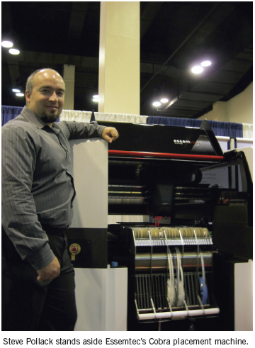
As is typical of regional shows, there was not much new in the way of technology. What did make the trip was worth seeing, though. DEK (dek.com) debuted its ProActiv squeegee, which oscillates during the print stroke in order to pack more paste into the apertures. My old friend Phil Zarrow points out that the concept isn’t exactly new – roughly 25 years old, perhaps – but sometimes good ideas take awhile to find their place. Essemtec (essemtec.com) is beta testing its Cobra system, scheduled for released in January. It features 220 inline intelligent feeders that can be changed (“hot swapped”) during production and 30 µm accuracy at 3 Sigma.
Aqueous Technologies (aqueoustech.com) debuted its Trident One Shot system, the lowest cost defluxer the company has ever manufactured. It offers fill-and-drain for low-volume applications, and uses a minimal 4 oz. of chemical every cycle. Mirtec, which sold an MV-3L desktop AOI system at the show, introduced its ISIS system with five 10-Mp top-down/side angle cameras.
Those who blanch at the thought of placing 01005s better sit down. Assembléon’s (assembleon.com) Greg Berry, global director, medium volume solutions, talked about the next-generation of chip packages: 005005 (or metric 0201). Half the size of an 01005, they should reach production within two years.
There was more than a little handwringing over the prices of tin and other metals, which at press time were skyrocketing. Some materials vendors intimated that China may be holding on to stocks, as it has cut its export quotes by 10% for 2011. On the product side, Cobar (cobar.com) president Stan Renals mentioned three new fluxes are coming, probably by March. FCT Assembly (fctassembly.com) has completed a study on paste shelf life that revealed certain products can last up to nine months and can be exposed to air for up to 24 hr. without degradation. President Tetsuro Nishimura proudly showed photos of Nihon Superior’s (nihonsuperior.co.jp) new R&D center in Osaka, Japan.
There were a few notes to share on the qualification side as well. Acculogic (acculogic.com) showed its ThermalScan product that features an IR camera to scan the board, conduct a thermal signature and show hot spots. SolTec Electronics (soltecelectronics.com) is putting decapsulation specialist Don Davis’ background in failure analysis to good use through a new non-destructive service to help EMS companies determine whether chips are counterfeit. DivSys (divsys.com), a new company run by former managers of Diversified Systems, discussed its third-party bare board qualification services.
Juki (jas-smt.com) president Bob Black said the leads were much better than last year. Juki is now back to its 2007 sales and production levels, he added. Dynatech’s (dynatechsmt.com) Mike Foster, who handles Samsung’s placement equipment in the US, added that machine backlogs reached 600 this year. Mirtec’s North America unit (mirtecusa.com) had its best October ever, and revenues are up about 70% over last year in Korea.
One last note: As he received the SMTA Founders Award, given to individuals for exceptional contributions to the industry and support of SMTA, Libra Industries (libraind.com) founder Rod Howell made an extraordinary gesture with a $5000 donation to the Charles Hutchins Grant. The grant underwrites the costs of a student doing post-graduate work in the fields of electronics packaging or assembly. And the SMTA has renamed its best paper award in honor of the late Rich Freiberger, a former director of the trade group and one of its most avid supporters. A nice touch.
Mike Buetow is editor-in-chief of CIRCUITS ASSEMBLY; This email address is being protected from spambots. You need JavaScript enabled to view it..
The cross-functional decision team cares about solutions, not flash.
Our economic roller coaster is not the only face of uncertainty in the electronics manufacturing services account acquisition process. Traditional marketing channels are continuing to evolve. Media companies and trade show organizers are consolidating. Publications are disappearing (or reappearing with new looks). More content is delivered online.
All this change has disadvantages. EMS has always chased a niche audience: the cross-functional decision team. Most of these people aren’t sitting in cubicles surfing the net, reading promotional emails, frequently attending industry trade conferences or scheduling meetings with the salespeople hanging out in their lobby. Over the past several years, they’ve seen their departments downsized and budgets cut while their workloads and performance targets increase. They aren’t interested in flashy messages or slogans, but they are interested in solutions that address the challenges they face.
While consolidation continues in EMS, more available options for reaching the cross-functional decision team ensure it constantly is bombarded by messages from far more EMS providers than it needs to explore. Relevant messages get lost in the “noise.” Worse, methodologies for really understanding true readership or attendance at an event are deteriorating. The speed at which publications and trade shows change focus or venues makes it difficult to assess accurate readership or attendance prior to purchasing ads or leasing booth space. That said, properly structured, the ability to track readership of a given ad or white paper is far better than it was even five years ago. Trade show data for a show that stays in the same place year-to-year are also good.
The rules of the game haven’t changed. EMS is still an educated sell. If you can reach the decision team and deliver a focused message that clearly addresses how your company will solve their problems, you will compete on quality of solution rather than price alone. In the absence of a clearly defined solution, OEMs select the contractor that represents the safest choice in terms of lowest price, position in the industry, or geography they are told to source. The trick is selecting the best channels for message distribution: Typically, that is an integrated sales and marketing strategy.
While publication selection remains highly variable depending on services sold, industries targeted and decision team member focus, there finally is a little clarity in the trade show realm. How long that will last is anyone’s guess because the economy will ultimately determine what show attendance looks like in 2011. I’ve just come back from IPC Midwest and SMTAI. Since I’ve been critical of the number of shows in past columns, I think this is a good time to discuss some positive trends I’ve seen in these venues.
This year IPC combined with Canon Communications (now UBM Canon, thanks to a recent merger) to present Electronics Midwest. In my opinion, this was a great move for EMS companies, as well as attendees of both shows. Having IPC Midwest run in Schaumburg, IL, while Canon’s MDM Midwest and associated shows ran simultaneously 20 minutes away in Rosemont was confusing to attendees and split the potential attendee base. The combined shows use the conveniently located Rosemont Convention Center, present a strong technical conference and have enough diversification in exhibits to attract good potential prospects for EMS providers. The MDM series of shows reaches the EMS decision team far better than any IPC show. However, the IPC-led technical conference does a far better job of delivering “must see” content to technical members of the decision team. Most important, overworked decision teams have a regional venue where they can look at a variety of exhibitors and catch up on relevant technical and business issues.
Former IPC Midwest exhibitor comments suggested that leads were significantly better than the prior year’s split show. Compared to Apex, the latter is more of an equipment show than a venue likely to attract a strong number of pure EMS prospects. As with SMTAI, Apex’s technical conference provides networking opportunities with OEM personnel that may be able to provide insight to their companies’ sourcing plans, but neither show is a strong EMS lead-generating option. Electronics Midwest stands as a good regional play for reaching medical EMS prospects, with possibly some attendance from other OEMs looking for equipment or attending the conference.
Traffic was up at SMTAI this year, and a number of smaller equipment vendors exhibited for the first time. While not a great EMS show, it is a good networking venue. While it is hard to predict what next year will bring as the show moves to Dallas, I think the move is positive.
Overall, traffic at all electronics industry shows increased this year. Part of this is economic recovery. Part is more focused show options. And probably the biggest part is component allocation and uncertainty over what the economy will do next. People are networking and listening in higher numbers than last year. It is a good time to put out a strong message: Trade show exhibits and conference presentations for now are viable options.
Susan Mucha is president of Powell-Mucha Consulting Inc. (powell-muchaconsulting.com), and author of Find It. Book It. Grow It. A Robust Process for Account Acquisition in Electronics Manufacturing Services; This email address is being protected from spambots. You need JavaScript enabled to view it..
To attract real talent, we must commit to look and act like a world-class tech industry.
One of the more enjoyable activities this time of year is to get together with old friends and business colleagues. Maybe it’s a sign of age, but it sure seems that I know more people who “were” in the industry than who “are” sharing the trenches with me. It's concerning to realize how many bright and talented people have left and how few seem to be stepping in to take their place.
The talent drain is real. Our industry was created by technologically bright people with entrepreneurial skills and business savvy. They developed processes, created products and forged an entire industry. Between normal aging and shrinking numbers of companies in historic industry epicenters, the talent pool is, shall we say, thinning.
For years the industry has contracted in terms of employees and shifted toward “production” economies (vs. “innovation” economies). With the West relatively light on companies and the East’s uncontained growth, developing a solid talent pool that is mobile and readily available has become far more difficult. So many new businesses focus almost exclusively on ultra high-volume applications, and the game is truly changing.
Where are the industry leaders of the future? Not the financial or sales leaders, but industry technology leaders – the people who understand materials, application and process, and know how to make them all work together? And when we find them, how are we going to keep them?
If recent history is any indicator, we have our work cut out for us. For an industry that has been the poster child of “high tech,” technical people are scarce. Most companies – OEMs, EMS and fabricators – are managed by generalists. Management may know how to engineer a balance sheet, but they are not competent in shop-floor processes and end-customer applications that drive our industry. Most companies have sales staff that boast technical degrees but have never held positions on the technical side, with the possible exception of their first job. The days of the designer or process chemist starting a company are long gone. Ditto for the founding entrepreneurs who may have had their management skills honed while with Tier 1 entities, but who had enough faith in their technical expertise to start or manage companies that redefined process technology.
Do you need the same level of technological talent today as you did back then? Maybe one reason margins have eroded is that the sales and marketing model has shifted from technological expertise to the more commodity-focused “don’t ask, don’t tell” cyber-portal approach. Those selling to technology-driven applications and customers may actually need a technologically competent sales staff! Ditto for manufacturing. When acceptable yields are measured by process excellence, you need a technologically focused staff to balance capability with first-pass yield.
How can we replace the retiring technical ranks? I have heard many voice frustration over finding talent and few who have had great success. Even for large companies, hiring and retaining top talent is daunting. For those near the bottom of the industry pyramid, the financial wherewithal to hire can be close to impossible.
Emerging companies in Asia, where educated engineering talent is readily available, have it easier. These companies just need to provide the environment to learn, experiment and contribute. Like any business, the entry staff needs to feel their contributions will be valued, with a path for promotion. And yet, the dynamic environment of technology combined with emerging market offers provides the setting for high turnover and low employer/employee loyalty. The sheer numbers of available talent may look appealing, but with those numbers come challenges too.
Mature markets – regions that are less dynamic but still demand excellence – have a different challenge. Our challenge is twofold: to believe in your company, and to inspire new and veteran employees to make a difference, today and long-term.
That is only the beginning. Why leave a position at an established company in a different industry or graduate from college only to work in a company that looks physically and attitudinally dead? To attract talent means making the commitment to look and act like a world-class technology industry. Too many companies look like old mills about to fold. And you often act how you look. A little enthusiasm and some elbow grease can change the appearance and attitude in a way that will attract talent.
Which brings me back to those who are no longer in the industry. Too many left not because they wanted to, but because they were victims of kneejerk budget cuts by non-technical management of struggling companies. It is clearly documented that many of those struggling companies failed because they did not have technically competent people to round out the capability and make the improvements needed to compete. More than ever, we need technical people in all facets to ensure we remain a value-add industry.
We can’t outsource engineering, CAM services, process management and all else that makes up our technical value-add quotient without, at some point, losing control of our destiny. Sans a concerted effort to attract, develop and reward technologically talented people, innovation, profitability and overall success will become more elusive – no matter where you are located.
Peter Bigelow is president and CEO of IMI (imipcb.com); This email address is being protected from spambots. You need JavaScript enabled to view it.. His column appears monthly.
The past 12 months have been highly transitional for the printed circuit industry. After years of vast migration of manufacturing to Southeast Asia, some stability has been achieved, and in some cases, programs are coming back to North America and Europe.
Even in China, the upheaval has been pronounced, as companies flee the southern coastal region for more inviting (read: lower labor cost) climes inland. Still, given the uncertainty that comes with volatile swings in orders, shaky financial footings and scarce employment, it’s no surprise many workers cast about as if they have been in a war zone.
Some literally have. And if a pair of New England companies has their way, hundreds more will soon.
Veterans Assembled Electronics (vaellc.com) is a service-disabled veteran-owned small business that trains, certifies and starts veterans on careers in electronics manufacturing. Founded last year, VAe has teamed with the Department of Veterans Affairs VR&E Program to provide a six-week electronics training program, under which veterans obtain the five major IPC certifications.
Founder John Shepard, who has spent 30 years in the computer and biometrics industries, says he originally set out to assemble a team who could win a piece of the millions in Department of Defense contracts set aside for disabled veterans. In the face of uncertain pricing and component availability, however, he shifted VAe’s model to training veterans to do that work. A US government plan known as the Vocational Rehabilitation and Employment (VR&E) VetSuccess Program (or Chapter 31) provides funding to train veterans whose disability otherwise interferes with their ability to be employed. Shepard received authorization by the VA for the training, and while initially he planned to offer training in-house, he quickly saw the value in leveraging existing infrastructure.
Enter EPTAC. Shepard approached the longtime IPC training center, recalls president Mark Pilkington, pitching certification for disabled veterans. “That first day, we talked for several hours. He needed a partner to help execute this. I thought it a viable opportunity to give back. You can start to lose your perspective in making a difference. This is a little more tangible: You can see the progress [of the students]. They are self-sustaining. They have contributed to serving the country. It feels good to do something worthwhile.”
EPTAC, which cut its typical training fees, provided the VAe students with the whole gamut of certifications, from basic hand soldering to IPC-A-600 qualification. Working with novices was daunting at first, Pilkington admits. “We train business to business. Most of the people have a background in electronics manufacturing. These guys were brand new to the industry. It was kind of intimidating, but they performed really well. IPC-A-600 is a difficult program, but they made it through. “And when they are done,” he adds, “they have every single certification IPC has to offer. It’s the first time I’ve given so many certificates to one individual.”
To date, seven vets have passed the program, and the placement rate has been high. If Shepard’s vision is realized, some 300 veterans will be certified in all five programs over the next 24 months. But he is measuring success not on the number trained, but the number hired and the sustained value they deliver to the employer.. To that end, Shepard has been in contact with Jabil and Plexus about their future needs, reasoning that he could help provide a steady flow of certified operators. “We would do the training at our expense specifically to their headcount and criteria, so they get a highly trained mature veteran with all five certifications for bare boards through rework and hand soldering. They won’t pay any [additional training costs]; the VA pays us to train that veteran. It’s a great opportunity for the veteran and for the employer.”
Pilkington says the arrangement has given him new admiration for EPTAC’s instructors. “Their ability to deliver this material to people who had no previous exposure to it and successfully get them through the certification has been satisfying,” he says.
Shepard, who came home from combat in Vietnam with a variety of ailments from hearing loss to a knee injury, sees opportunity. There are dozens of VAs and thousands of disabled vets across the country, and each one he trains and places is further validation of his vision.
The tragic suicides of so many workers at Foxconn’s China plants cast a harsh light on the conditions at electronics factories. Yet the swell of criticism helped force wages higher, and may over time spur better lives for hundreds of thousands of lower-paid employees in a variety of industries. We may well look back on 2010 as the Year of the Employee. If so, VAe and EPTAC will have helped make it so.
Rewarding experience. Entries are being accepted for the annual NPI Award, given to the best products for design, fabrication, assembly and test introduced in the past year. We are pleased to announce the 2011 NPI Award will again be presented at Apex. Visit circuitsassembly.com/cms/npi-award or pcdandf.com/cms/component/content/category/229-npi-award for more information.
For best results, know where to put solder mask, final finish and components.
Fine-pitch devices and automation levels are resulting in greater board density. There are mechanical and logistical limits to how far these trends can go, however, and the following best practices will help ensure that an SMT device is manufacturable.
For fine-pitch devices, designers must be careful to ensure that no natural bridges occur. A natural bridge is a clear, straight track between leads. This creates a trace over which solder can (and likely will) run when soldered (Figure 1). Although the result is not technically a defect, it appears as one to automated and human testers. This causes delays and additional manual (i.e., expensive) intervention to check. To avoid natural bridges, traces should be designed to route from the ends of pads, rather than using direct, straight connections.
Vias are holes drilled through layers of a PCB and plated to connect the layers of circuitry. Two design practices should be observed regarding vias and ball grid arrays:
Always mask vias under BGAs. Solder from the paste or balls on the BGA may come into contact with the via, creating a defect. Rework is problematic, as more heat is required to melt the solder. To avoid this situation, mask vias under BGAs with solder resist.
Avoid placing vias in pads. If a via is placed where a device is to be mounted, solder can run down the via, making rework difficult and reducing control over the solder joint volume.
Always ensure that copper pads define the solderable area, rather than using mask-defined pads. The mask application process is not as well controlled as the copper definition process, and defects are more likely to result.
Balance the thermal mass on leads of smaller devices, especially 0402s. Thermal imbalances can cause a defect known as tombstoning. In such cases, as one end of the device reaches temperature faster than the other end, surface tension on the molten lead causes the device to stand up on end.
Also, to achieve a flat PCB finish, organic surface protectants (OSP), electroless gold plating, or immersion tin finishes should be used on fine-pitch and BGA devices. This helps prevent defects such as open circuits on devices that contain many coplanar leads.
Solder resist dams of 0.003" are required, particularly on fine-pitch SMT devices. Omitting these dams increases the risk of short circuits through bridging between leads. The dams between these leads must be a minimum of 0.003" to be manufacturable by modern PCB fabrication processes.
Wave Soldering
The most economical method of soldering plated through-holes on SMT boards is with a solder wave machine (rather than manually). To help ensure that a board can be successfully passed through the wave, the following best practices should be observed.
Problems in manufacturing arise when a mixed board is heavy. Proper support and clear edges for stiffeners help avoid such issues. “Submarining” is a term used to describe the difficulties encountered when a double-sided board with inadequate support is put through wave solder. The board may sag, permitting solder to run across the top of the board and ruin it.
If a double-sided mixed-technology board is so dense that the above guidelines cannot be observed, a special fixture called a selective wave fixture into which the board is snapped can be used. This masks the bottom-side surface mount from the wave. To do this, there must be sufficient clearance (0.1") between the PTH pins and solder-side SMT so that the SMT can be masked by the fixture.
Keep in mind that fixtures add cost to the product, and it is best to avoid designs that require these. Several fixtures are required (at several hundreds of dollars each), and they have to be cleaned, loaded, unloaded and occasionally replaced.
Careful SMT pad design should be employed on the solder-side of a board. This includes thieving pads and toe pads, both necessary for successful wave soldering. In addition, components on the board should be oriented so that the solder joints are not shadowed as the board moves through the wave solder.
In all designs, snap-off materials should be designed on the edges of the board (Figure 2). These help support the board through the wave machine and can be removed after soldering. They also permit conveyors and clamps to function properly.
In some cases, titanium stiffeners can be used (provided there is sufficient clearance on the board) to help make the board more rigid. Both techniques require additional labor and therefore, add cost to the final product.
George Henning is vice president of manufacturing at OCM Manufacturing (ocmmanufacturing.com); This email address is being protected from spambots. You need JavaScript enabled to view it..
A common signal encountering the asymmetry that created it can cause noise.
Those familiar with designing high-speed single-ended interconnects don’t have a huge leap to design high-speed differential pairs. Both types of interconnects require controlled impedance, minimized discontinuities, low loss and short stubs.
But, one important new problem can arise in differential pairs that has no comparable effect in single-ended interconnects. This new problem can completely swamp the differential signal at the receiver and can make the difference between a robust product and one that works with boards from some vendors but not others. We call this new effect “mode conversion,” and it is related to the nature of signals on differential pairs.
It takes two transmission lines to transport a differential signal. We call the combination of the two transmission lines a differential pair. The differential driver that drives a signal on a differential pair has two output pins that create two different voltages on each of the two signal lines, with respect to their common return path.
These two independent voltage signals are usually denoted by either V1 and V2 or by Vp and Vn or by V+ and V-. They are the voltages between the signal line and the adjacent return path on each line.
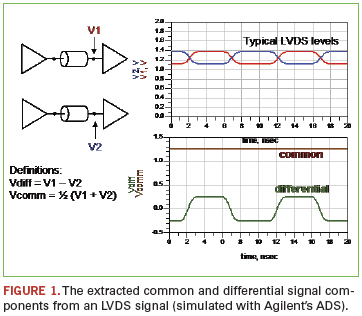
For example, Figure 1 shows two voltage levels for an LVDS-type signal. Voltage coming off the two signal pins of the LVDS differential driver is called a differential signal, but this is a lie. Not all the signal is a differential signal: There also is a large common signal component.
By definition, the differential signal component is the voltage difference between V1 and V2. The common signal is the average value of the voltage. When we apply these two definitions to the LVDS signal, we see the differential component has a very simple form, and, in this case, a common signal is present, but constant.
If the two signals, V1 and V2, are perfectly symmetric – the same values, but exactly opposite – the average value will always be constant, and there will be no modulated common signal. If there is any asymmetry in the two voltages that make up the two signals, either in their voltage levels or their relative timing, some of the differential signal will be transformed into common signal. This effect is mode conversion: any asymmetry of any sort between the two signals that creates common signal and distorts the differential signal. This can arise from asymmetry in the driver or asymmetry between the two lines that make up the interconnect. No amount of distortion of the differential signal path will cause mode conversion, provided whatever is done to one line is done to the other. Of course, the differential signal could be grossly screwed up, but if so, there will be no mode conversion.
A difference in the cross-section between the two lines that make up the differential pair would change the impedance the driver sees looking into each of the two lines, and this would affect the voltages launched into the lines and generate common signal.
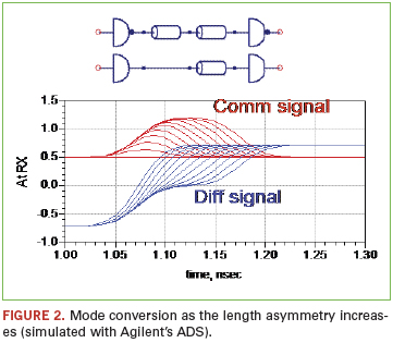
The most common source of asymmetry is a length difference between the two lines that make up a differential pair. It’s very easy to explore the effects of a length asymmetry on a differential signal using any circuit simulator that can perform a little algebra to show the calculated differential and common components of the signal (Figure 2).
As the length difference increases, the differential signal is degraded and a common signal is created. The most important problem with mode conversion is that the differential signal is degraded. Any length difference between the two lines in the pair will cause a time delay skew between them, resulting in some conversion of differential to common signal. And, this happens at the edges of the signal, which will directly impact the shape of the eye diagram.
A possible problem with the common signal arises if it were to get outside the enclosure of the product, on external, unshielded twisted pairs. It only takes about 3 µA of common current on external cables to fail an FCC Class B certification test. Less than 1 mV of common signal on an external unshielded cable will fail this test. That’s why every RJ45 connector to a cat 5 cable uses a common signal choke to dramatically attenuate common signals before they can be launched onto unshielded cable. However, if the common signal does not get out of the enclosure, it will rarely have an EMI impact. After all, every single-ended trace on a circuit board has a huge common signal without causing EMI issues.
Impact on Eyes from Mode Conversion
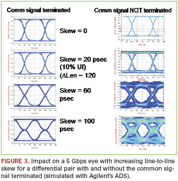
A more important secondary problem with mode conversion is that there will now be some common signal rattling along the differential pair. If it is not terminated, this common signal will reflect back and forth between the ends of the line. Since the receiver is sensitive to only the differential signal, rarely will the common signal cause a problem for the receiver.
However, if this common signal, in reflecting up and down the line, encounters the same asymmetry that created it, some of this common signal may convert back into differential signal, and this new differential signal, asynchronous with the initial differential signal, will be picked up by the receiver and look like random noise. Figure 3 shows the impact on a 5 Gbps PRBS eye for different line-to-line skews for the two cases of the common signal terminated and not terminated. When it is not terminated, the differential noise increases over the entire eye. When the common signal is terminated, it will not rattle around and will not contribute to asynchronous differential noise.
Terminating the common signal does nothing to prevent mode conversion and the distorting of the differential signal; it just keeps the reflecting common signal from distorting it further. Terminating the common signal will result in a cleaner eye, and the same amount of mode conversion will have less impact with a terminated common signal than without.
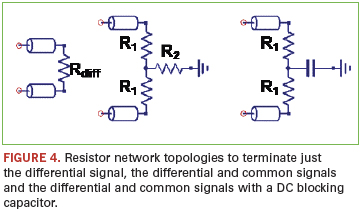
In all high-speed serial links, it is critical to terminate the differential signal, and this is always done with a resistor across the far end of the differential pair. The common signal, when reaching this far end resistor, will still see an open and reflect. To terminate both the differential signal and the common signal requires not one resistor but three (Figure 4).
To terminate the differential signal at the far end, R1 must be the odd mode impedance of the differential pair, typically close to 50Ω. To terminate the common signal at the end of the line, the parallel combination of the two R1 resistors in the series with R2 must be the impedance the common signal sees. After a little algebra, the value of R2 is found to be 0.5 x (Zeven – Zodd).
In loosely coupled pairs, the difference between the even and odd mode impedances is very small, so R2 is on the order of 1 to 5Ω. With this resistor network, the drivers will see an impedance of about 25Ω to the return path for the common signal. This will often mean a very high power dissipation, disastrous in many applications.
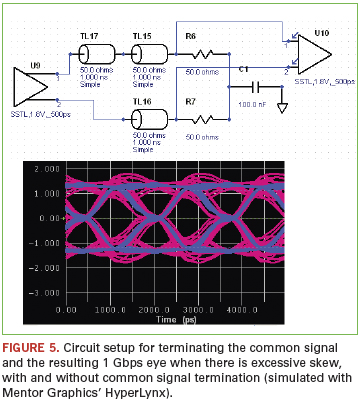
To prevent the DC power consumption but still provide an adequate termination for the common signal, a DC blocking capacitor is often placed between the center tap of the resistors and the return of the common signals. This network will terminate both the common signal and the differential signal. The implementation of this network and the resulting eye of a 1 Gbps PRBS signal with and without the common signal terminated are shown in Figure 5.
If there is so much asymmetry to distort the differential signal to worry about terminating the common signal, the way to fix this problem is to first eliminate the asymmetry at the source, then worry about terminating the common signal.
Too Much Skew?
Do not confuse line-to-line skew in a differential pair with jitter in the eye diagram. They are not the same. In fact, even when the skew is as long as 10% the unit interval, the impact on jitter in the eye is barely discernable.
It is common for high-speed signaling protocols to set a limit on the total acceptable line-to-line skew in a channel as less than 10% the unit interval. This includes all sources of skew, such as in the driver, the packages, the connectors, cables and the circuit board traces.
For a 1 Gbps signal, the unit interval is 1 nsec and a total skew spec might be 0.1 nsec. If this is all due to a length difference, using roughly 6 in/nsec as the speed of a signal, this suggests the total length difference that could be tolerated is 0.6 in. But, this is to be allocated to all circuit elements. If the board is allocated 10% of this total skew budget, the spec on the length matching for the board interconnects would be 0.060". As the bit rate increases, the total length skew allocated to the board would decrease.
For example, at 5 Gbps, this would be a total length skew limit of 0.012". When it is no longer free to match line lengths in a differential pair to this close a length, the skew budget would be renegotiated, or reevaluated. After all, a total skew of more than 10% the unit interval can be tolerated in many designs before the jitter becomes noticeable. At 5 Gbps, this is a length difference between the two lines in the pair of 0.120".
A second source of skew comes from the difference in speed between the signals in the two lines, as due to an asymmetrical dielectric distribution. This arises when one line in a pair sees more glass bundles than the other line and a higher Dk value, and travels slower than a signal in the other line.
This “glass weave”-induced skew is statistical in nature. It comes about due to the random chance that one line overlaps a glass bundle, while the other line in the pair sees a more resin-rich region. The magnitude of the effect depends on many uncontrollable factors, such as how well aligned the routing trace path is to the glass weave axis, the local variation in the Dk across the glass weave bundle, the pitch of the glass weave and the pitch between the two lines in the pair.
Controlling this source of mode conversion is about risk reduction. One approach is to keep your fingers crossed and hope for the best. Some designers have found this an adequate risk reduction strategy at 2.5 Gbps and hope it will also work at 5 Gbps.
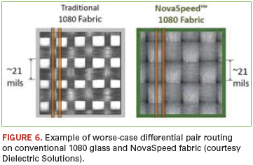
Another approach is to route the two lines in a pair on the same pitch as the glass weave. In typical 1080 or 2116 glass yarn, the weave pitch is about 0.021" along one axis. Routing the two lines in a differential pair on a 0.021" pitch will increase the chance the two lines see the same local Dk environment – either both resin-rich or both glass-rich.
Yet another approach is to use a glass yarn that is more uniform (Figure 6). In this case, the Dk does not vary nearly as much over the surface of the board, and the weave induced skew is dramatically reduced.
There are routing solutions as well: Don’t route along the glass wave axis; rotate the artwork relative to the edge of the board, or route with zigzags. All these solutions are to try to decrease the change of creating glass weave-induced skew.
As with so many signal integrity effects, problems get worse as data rates increase. While 1 Gbps systems have a high tolerance for skew-induced mode conversion, a 5 Gbps system is much more sensitive. Design approaches for 1 Gbps systems may not work at 5 Gbps, and it is important to reevaluate the design processes and constraints to verify robust performance in your next system design. This is why understanding the nature of the mode conversion problem, its root cause and the solutions available in your toolbox is more important each day. As we know, as speed goes up, luck goes down, but the more you know, the luckier you get. PCD&F
Eric Bogatin, Ph.D., is a consultant and founder of Be The Signal (bethesignal.com); This email address is being protected from spambots. You need JavaScript enabled to view it..