Save real-estate using digital pre-distortion to linearize power amplifiers.
In multiple channel applications of the next-gen communication systems, it is often desirable to develop an antenna system to combine many of these antennas into fewer antennas by using modern wide-band antennas and power amplifiers for multiple transmitters. This can be extremely helpful because in many locations, the deck of a vessel for instance, real estate is so limited it is not possible to mount every antenna required for each possible frequency range and application. Through the use of wide-band antennas and power amplifiers (PA), the power, weight and the amount of real estate consumed by antennas and electronics can be significantly reduced. This would permit smaller vessels to have the same capability as larger vessels and increase their tactical advantage.
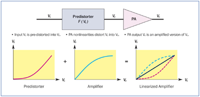
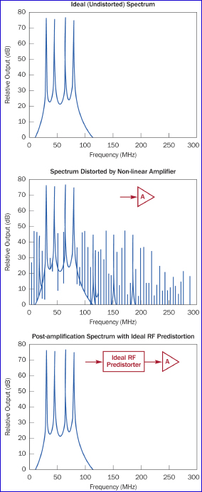
To maximize efficiency, modern wide-band power amplifiers must operate in a nonlinear region. However, this creates large variations in the instantaneous output power, a condition described as high peak-to-average ratio (PAR). As a result, signals are distorted. To compensate for this distortion, linearization techniques must be applied to minimize spectral re-growth or intermediation products created by the nonlinearity of wide-band amplifiers. A method called digital pre-distortion is used to distort the signal prior to the input of the power amplifier. The signal is distorted such that the composite output of the power amplifier appears to have linear amplification over the desired frequency range, without distortion. Figure 1 shows the digital pre-distortion method, which is used to linearize power amplifiers over very broad bandwidths. Figure 2 shows an example of the effects of power amplifier nonlinearities on a transmitted spectrum and the potential spectral benefits of applying digital pre-distortion.
Figure 1. Linearization of a PA using digital pre-distortion. Courtesy Northrop Grumman.
Figure 2. a) Ideal (undistorted) spectrum; b) spectrum distorted by nonlinear amplifier; and c) post-amplification spectrum with ideal RF pre-distortion.
The effectiveness of digital adaptive pre-distortion is that it enables high power amplifier linearization of spectrum to combine multiple transmitters across entire VHF and UHF ranges. Harmonic or intermediation products are reduced by more than 15 dBm. Additionally, cancellation improves receiver dynamic range. In the proposed antenna combining, pre-distortion is performed by digital signal processing techniques using open architectures that enable reduced cost and increased flexibility of the system. System level control, switch control for communication equipment selection, oscillator control and antenna selection are supplied by a standard single board computer utilizing a Versa Module European (VME) bus-based chassis. Also, populated in this VME chassis is a software-defined radio board, a wideband transceiver board consisting of field-programmable gate arrays, analog-to-digital converter, and digital-to-analog converter (DAC).
The digital signal processing for the pre-distorter is performed by FPGAs using a down converted and sampled signal. The signal is mixed down to an intermediate frequency for sampling by an analog to digital converter for input to the FPGA for filtering. Then the filtered digital data are sent to a DAC, which is then mixed back to the carrier frequency for input to the power amplifier. Thus an undistorted signal is output to the antenna for improved signal integrity. If the bandwidth of the pre-distorter is large enough, then multiple communication systems within the same frequency range can be combined to utilize the same amplifier and antenna set. Some precautions need to be taken to ensure the communication systems are not utilizing the same frequencies, and have ample channel separation. Since the pre-distorter is implemented in reconfigurable hardware FPGA, modifications to the pre-distorter are possible even after the system has been produced.
ACI Technologies Inc. (aciusa.org) is the National Center of Excellence in Electronics Manufacturing, specializing in manufacturing services, IPC standards and manufacturing training, failure analysis and other analytical services. This column appears monthly.
Budget cuts will directly affect the US PCB supply chain.
With the US deficit running above $13 trillion and continuing economic uncertainty, the federal government has begun instituting significant cuts in military programs. These cuts will have a direct effect on the North American interconnect industry, both PCB fabricators and assemblers.
The just-issued Quadrennial Defense Review (QDR) foresees major cuts across the board in defense hardware. To some extent this includes already announced cuts, such as reductions in F-22 fighter plane acquisitions (to 180 total airframes) and to F-35 aircraft as well. Inventories of aircraft such as the A-10 attack plane, B-1B bomber, and the venerable B-52 also will be reduced.
At sea, while the government states its commitment to a 313-ship Navy, analysis of projected budgets over the next 10 years suggests that, between replacement construction and new classes of ship, the US Navy more likely will be reduced to approximately 270 vessels. The ASDS submarine program is in jeopardy, while carrier battle groups are projected to shrink to 10 from 15. Overall capital budgets for military programs may drop as much as 30% over the next five years, much of this in electronics.
Cost overruns on major programs have been horrific as well. The Littoral Combat Ship (LCS) program has in three years’ time ballooned from $220 million/ship to $480 million/ship – and that’s before the contracts have even been awarded. The F-35 fighter program budget has increased almost $100 billion over the past decade, and development remains 2.5 years behind schedule. While some of this is related to a massive flow of change orders and technology development issues, much of the problem lies with a hollowed-out workforce and knowledge base. These overruns cut further into available funds for new hardware. Former Defense Secretary Donald Rumsfeld entered office with a mandate to streamline the Pentagon procurement process. Instead, his efforts were devoured by the military-industrial complex.
What will be the effect on the US interconnect manufacturing base? The North American industry has shrunk from a high of $10 billion in 2000 to approximately $2.8 billion today. One reason it did not shrink further was the cushion of defense electronics. Many manufacturers went through the rigorous steps to qualify for MIL-PRF-31032, MIL-55110 and other standards, and the shift from commercial to military production kept many companies alive through the recession. These trends will require manufacturers to anticipate, adapt and innovate.
At the same time, many military systems have been commoditized, some successfully, others not so much. In other cases, subsystem manufacturing has been shifted offshore either because of commercial off-the-shelf technology (COTS) programs or efforts by some contractors to reduce costs.
Bluetooth and iPhone-type applications in military applications have been growing exponentially, but the loss of the handheld market to Asia means that much of the hardware technology has migrated offshore. This will have a long-term effect on programs such as Land Warrior. Because of security concerns, several major defense contractors have established secure communications projects, but these will have minimal impact on the demand for interconnect product.
Indeed, the proliferation of consumer-level high technology is amazing. The capabilities of handheld devices – whether for communications, data recording, conversion and transmission, or imaging – are beyond Buck Rogers. The mythical Star Trek Tricoder today is close to reality. And yet the defense technology establishment has lost its connection with the underlying electromechanical roadmap.
Discussions with key defense interconnect manufacturers have established there are significant opportunities, especially at the leading edge. Yet there is cognitive dissonance at the top. The role of enabling technology, especially at the interconnect level, has been forgotten. In addition, technology security has become a significant issue.
On the security side, the cyberwarfare arena has, according to many reports, been underfunded and misunderstood. Recent headlines in the telecommunications market, where governments have expressed deep concerns about potential technology breaches when purchasing networking gear that may be susceptible to trapdoors, viruses, and remotely executable programs, illustrate real-world issues with non-trusted components and hardware.
From every challenge springs an opportunity. There are real interconnect hardware-based solutions available both to protect systems and provide enhanced security, not only from penetration, but of intellectual property.
High-density interconnect combined with embedded active and passive component technology offers a security platform only dreamed of even five years ago. If critical IP or security is on an embedded chip, it can be shielded both physically and electronically, increasing the difficulty of corruption by orders of magnitude. Hard encryption keys can be made even more secure. Not only that, it makes a better, more reliable, more cost-effective product. Ask Apple or RIM or Sony.
Espionage efforts against the North American technology base have cost our national defense trillions of dollars when considering the loss of advantages in fields ranging from nuclear weapons design to aircraft design to under-the-hood applications such as the interconnect. Even simple applications such as software keys can be made more secure using a technology that, while slightly more expensive, saves much more on the back end. Think of the cost of the recent Wikileaks scandal. If adversaries cannot penetrate systems and/or copy technology or documents, how much is that worth in the long run?
The downsizing of the military electronics market is virtually inevitable. However, there is a chance to redefine and rebrand the interconnect, and with it, to add real value to the end-user. The North American industry, for once, can build on the experience of others. The inflection point for economically competitive leading-edge technology with reduced risks of implementation is close at hand.
The 1990s saw massive outsourcing and then offshoring based on the commoditization of the interconnect. The reality even then was that the interconnect is the cardiovascular system of every single electronics device in the world.
The electronics interconnect industry owes much of its life to the military sphere when OEMs such as Ford, Philco and Motorola found new and vital applications such as artillery fuses during World War II for what were then called printed wiring boards. Integrated design, engineering and manufacturing was critical to the success, and to an extent, to the winning of the war. We may have come full circle. Defining the interconnect as an active component changes the game and will require a much closer relationship between the manufacturing floor, the packaging designer, and the systems designer. This is one potential avenue for the interconnect industry, but will require significant re-engineering of management thinking and investment in plant and equipment.
However, the payoff in jobs, in productivity, in profits, is real and demonstrable. Over $3 trillion was spent in stimulus funding and to stabilize the US banking system. Virtually every dime spent, though, has been to maintain the status quo. We must spend our defense dollars especially wisely today. At the same time, innovation has taken a massive hit. Innovation will help grow our economy for the long term, and electronics are at the heart of the modern economy. The interconnect is the heart of the electronics device. Where better to invest?
The alternatives are not especially palatable. While electronics content will continue to grow as a percentage of overall systems cost, the hardware portion has to a great extent plateaued. In addition, with commoditization and design rules that are in many cases 30 years old, where is the potential for profit that keeps a company viable? Where will growth, or even stability, come from in a declining market?
Matthew Holzmann is president of Christopher Associates (www.christopherweb.com); This email address is being protected from spambots. You need JavaScript enabled to view it..
Some finishes are more resistant than others, but lack of a standard hinders testing.
A coworker asked yesterday why he was chosen to work on a defect that was less than a fraction of a percent in occurrence. It was like finding a needle in a haystack, he said. I know he was looking for sympathy, but I could not offer it, as my entire team has been working on creep corrosion for the past four years. For some, creep corrosion also occurs at less than a fraction of a percent defect rate. There is no industry standardized test to replicate it, and during the onset, the only thing known was that it predominately occurred in paper mills, fertilization plants, tire factories and car modeling studios. The answer to the question is even one unhappy customer is reason for concern.
When this column was turned over to me by John Swanson, he wisely instructed me not to tackle anything crazy on my first attempt. “Nothing like creep corrosion,” he said. This is the day I offer about 1000 words on the matter. I can and will talk at great lengths on this subject, so catch me at the next conference for the full dissertation.
Creep corrosion is a migration of copper sulfide across a circuit board. The SEM and EDS images (Figure 1) show a section of an annular ring. The pad is plated with silver (green) creep corrosion growing over the soldermask. The creep analyzes as rich in copper (red) and void of silver. Additional EDS mapping explains the creep area also is rich in sulfur.
Figure 1. SEM (left) and EDS photos of annular ring show creep corrosion (in green) growing over soldermask. The creep analyzes as rich in copper (red) and void of silver.
The defect reveals itself as an electrical short or open. Shorts occur when the volume of migrated copper has reduced the volume of a copper trace or via. A short occurs, of course, when copper sulfide travels to its neighboring trace or pad. For creep corrosion to occur, there must be exposed metal area in the final circuit. This is normally an area that was not soldered or not completely covered by solder. The environmental exposure must be high in sulfur and humidity for the corrosion to manifest. As stated, the greatest challenge is that a standardized test does not exist to recreate creep. IPC conducts a biweekly meeting to attack this very issue. After researching the environments where electronics were located, even those expected to be “clean” (such as data storage centers), it was determined there is a lot of bad air out there.
Initial attempts to create a controlled test for creep corrosion will be conducted in mixed flowing gas (MFG) chambers. The test centers around Battelle Class 4 conditions, but with almost 10x the concentration of hydrogen sulfide. Battelle uses 200ppb of H2S. This test uses 1500 to 2000ppb. Also, the operating temperature will be increased from 35° to 40°C. Unfortunately, not every MFG chamber can handle these test conditions. Some detectors are not calibrated to measure high levels of sulfur properly; some equipment cannot resist corroding under these conditions, and some lab managers just don’t want to expose their workers. At this point, a red flag should go up, and the alarm should be ringing in your head. It is difficult to accept, but our environments are getting worse, and these aggressive conditions are turning into reality. Electronics life expectations are increasing, so prolonged exposure will ultimately lead to high levels of corrosion on unprotected parts.
Of the surface finishes, immersion silver sees the greatest threat from creep corrosion. Topcoats have been formulated to mitigate creep. These topcoats act as barriers for the metal from condensation and contamination in the air. The topcoats are designed to protect both the silver surface and any copper metal that may be exposed. All these attributes have been achieved without detriment to the other functional performance characteristics of immersion silver. The immersion silver plus topcoat parts withstand all traditional MFG exposure. They even resist corrosion in more aggressive versions of MFG that veer from traditional conditions. Due to the limitations of some MFG chambers and the high cost of the test, OEMs and chemical suppliers have created internal chambers to recreate creep corrosion in a lab environment. These tests accelerate the conditions of mixed flowing gas and introduce sulfur in particulate form. Elemental sulfur is common to many of the environments where creep corrosion has occurred. It is a point that should be taken into consideration during test development.
The performance and acceptance of these topcoats has been well received, but some will hesitate until the real-world environments are truly understood and can be replicated. Questions are continuously raised about the ISA classification these coatings withstand, but perhaps the better question is, Should these classifications be revisited?
Lenora Toscano is final finish product manager at MacDermid (macdermid.com); This email address is being protected from spambots. You need JavaScript enabled to view it.. Her column appears quarterly.
Altium’s latest acquisition pushes PCB CAD to a new plane.
On Sept. 16, Altium (altium.com) announced plans to acquire Morfik Technology, a provider of cloud-based software applications, in an all-stock transaction worth an estimated AU$3.3 million. (The deal is pending due diligence.) The move is groundbreaking in that it reveals the full extent of the EDA company’s commitment to developing so-called cloud-based computing, whereby resources, including software, are shared on demand via the Web, vs. stored on millions of discrete company-specific servers.
PCD&F’s Mike Buetow spoke with Altium associate director of corporate communications Alan Smith the day of the announcement.
PCDF: How many employees does Morfik have? AS: Twelve total, nine of whom are software developers.
PCDF: When is the deal scheduled to close? AS: We expect this to be in the next few weeks, but we can’t be precise because of the due diligence that forms part of the process. Having said that, we are also accelerating the acquisition by bringing the Morfik development team into Altium’s offices to work with the Altium team on the development of the ecosystem infrastructure that we now plan to build into our software.
PCDF: Will it be accretive to revenues within the next fiscal year? AS: No, there’s no significant impact on Altium’s revenues.
PCDF: What specifically made Morfik so attractive to Altium? AS: Altium has been working with Morfik for a number of years, so Morfik’s attraction, based on what it has done with the development of tools to create dynamic cloud-based ecosystems, is well understood. It has to do with Morfik’s software engineering approach to the creation of object-oriented connectivity to the Internet. The two key phrases here are dynamic and object-oriented. These are essential for managing large amounts of content, which is what you have in electronics design: content down to the scale of individual components.
PCDF: What are the top technical challenges behind moving electronics design to cloud-based architectures, and how does the Morfik acquisition help Altium overcome them? AS: Two points: First, tactically, to help Altium establish its ecosystem today for subscription-based content delivery. Second, longer-term, Morfik is about developing cloud-based applications; these are the applications that will be the highest layer, running on the “sea of connected devices” in this ecosystem. If we are to deliver the tools and solution to help the designer move from device design to ecosystem design, then cloud-application development is a fundamental part of this solution. PCDF: When it comes to cloud computing, Altium is on record as seeing Google as being superior to Microsoft. Will customers have to choose a platform based on one or the other, or will electronics design in the cloud be platform-independent? AS: We don’t really know. Amazon (Amazon Web Services) is more significant than either Google or Microsoft because it provides a much broader industrial-scale infrastructure for cloud-based application that is provided as a utility service for organizations that want to provide these kinds of solutions.
PCDF: Would a cloud-based infrastructure force any change to the subscription model that most ECAD companies now rely on? AS: Not specifically. Cloud-based (Internet-based) models allow a real-time connection between customers and suppliers, as well as between customers and customers. This creates the possibility of having a much stronger and timelier value exchange between these parties. In the future, they can move the basis of software subscriptions away from being primarily based on software upgrades (new features, etc.) to a much stronger focus on content that can be delivered over time. In electronics design this includes component models, designs, price and availability from part suppliers, as well as feature upgrades being delivered in a “plug-in” model.
PCDF: Would cloud-based electronics design help resolve the persistent library and documentation issues that today cost designers extraordinary amounts of time? AS: An emphatic “yes.” Vastly improved data management is already a big focus of the next release of Altium Designer, in beta today, and cloud-based data exchange is a big part of this. Initial focus is on management of data between the board-design process, and the fabricators and assemblers of those boards, especially when the parties are in different regions and speak different languages.
How to ensure documentation for the EMS company is accurate.
Electronics assembly documentation includes files such as design schematics, assembly drawings, test procedures, bills of materials and more. Problems or omissions in this documentation result in delays and, in extreme cases, may lead to product deficiencies and quality issues. The following best practices will help ensure that documentation to be sent to the EMS company is in good order.
Documentation is typically provided to us in a .zip file that contains documentation related to details of the PCB, assembly work required, materials required, design schematics, test procedures, special instructions, and more. Ideally, the documentation files should be separated into discrete folders. As an EMS company, we prefer either:
A distinct .zip file for each type of data (e.g. schematics, bill of materials, assembly, test), or
One .zip with an embedded directory structure that keeps these types of data discrete.
The following are common errors related to manufacturing documents. Avoiding these errors will improve delivery time and quality.
CAD data. Not every contract manufacturer has the systems to handle CAD data. For those that do, accurate CAD data improve information flow and can reduce manufacturing time and design errors. For example, the manufacturer can query CAD data for accurate dimensions and other product details.
If using a third party for CAD layout, request the CAD layout data from that company. If producing CAD layouts in-house, follow these guidelines:
ASCII CAD is the preferred data format. ODB++ and GenCAD are acceptable alternate formats.
Ensure the correct version of the data is sent. Double-check the version, or rely on a rigorous documentation control program to ensure the correct versions are employed.
Send Gerber data in only one format, rather than multiple formats. At many firms, RS-274x is the preferred format for Gerber data.
Verify that the aperture data you send are correct; documentation sometimes contains aperture dimensions of “0”, requiring the CM to halt the process and request clarification.
Avoid sending redundant data, such as sending both Gerber files and apertur data containing aperture data separately. RS-274x Gerber files already contain the aperture data.
In the Gerber data or a separate PCB document, include specifications for copper weight, surface finish and laminate.
Schematics and drawings. Adhere to these three best practices when preparing schematics and drawings for a contract manufacturer:
Include PCB schematics. These tell the contract manufacturer how parts on a board are to be connected. CMs refer to these drawings to ensure interconnect is accurate and to solve problems, if they arise. EDIF format is preferred because an EDIF file carries intelligence that can be cross-referenced with CAD data and assembly drawings to speed debugging. PDF format is also acceptable, but does not contain intelligence. If the contract manufacturer will perform testing, providing a schematic is essential for debugging.
Include assembly drawings in the documentation package. An assembly drawing provides higher-quality information about board assembly than Gerber data.
Reference a workmanship standard to which the manufacturer must adhere. If special assembly steps or requirements exist, indicate these on the drawing. PDF format is acceptable for assembly drawings.
Bill of materials. Follow these guidelines when preparing BoMs for the contract manufacturer:
Send a BoM in only one file format. A spreadsheet is preferred to a text or PDF file.
Always include alternate parts in the BoM, as this ensures the benefit of lower pricing or reduced lead times on parts.
Always include complete manufacturer part numbers in the BoM; not doing so can cause delays.
Functional specification. A functional specification of how the product is meant to function is helpful if testing is being undertaken. This information cannot be conveyed by a schematic or CAD data. A functional specification should describe how the product is designed to work and its acceptable limits. This, in combination with the other documentation, allows technicians to understand the product quickly and move on to efficient testing and debug.
George Henning is vice president of manufacturing at OCM Manufacturing (www.ocmmanufacturing.com); This email address is being protected from spambots. You need JavaScript enabled to view it..
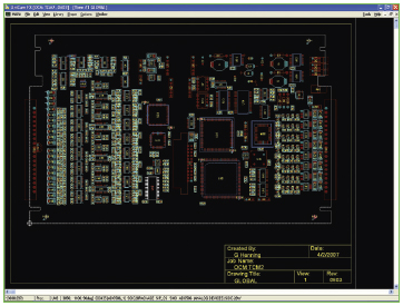
Figure 1. Working from the CAD system offers the best chance at accurate data.
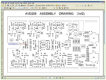
Figure 2. The assembly drawing provides higher-quality information about board assembly than do Gerber data and should be included.
How working in tandem applies to barbecues, car washing and PCB design.
Whether designing a PCB, cleaning the car or cooking a meal, we all look for ways to do things faster. Of course, at work there’s more at stake than, well, steak. Concurrent engineering introduces parallelism into our design process so that we can shorten, accelerate or recover our schedules. It permits different disciplines to have a positive impact on costs, quality and performance earlier in the design cycle – when it matters. A recent study by the Aberdeen Group found that best-in-class companies focus on improving communication and collaboration. They achieve this by working concurrently and collaborating across the extended PCB development team, and some report up to a 60% decrease in design cycle time.
Concurrent engineering is a widely used term and anyone who appreciates motherhood and apple pie will surely claim to practice it in their design process. I love my mother and enjoy apple pie as much as the next guy, but let’s get a bit more specific.
Consider two approaches to concurrent engineering:
A meal consisting of a salad and grilled hamburgers can be created quicker if one person makes the salad while in parallel another grills the burgers. With this approach, the time saved would be equivalent to the shortest time taken by either task. This is an example of independent concurrent engineering across disciplines: The two activities do not affect each other, but the overall schedule is shortened.
Two people can wash a car much faster than one person. Each person will not bother to wash what has been already washed by the other, but there will be overlap at the edges. With this approach, two people will not wash the car in half the time taken by one person, but they will definitely be much faster – say, a 40% elapsed time savings. This is an example of collaborative concurrent engineering within a discipline: Each activity is done in the context of the other and requires real-time communication in order to be optimal.
In PCB design, independent concurrent engineering is widely practiced because it can be achieved somewhat independently of a design tool’s capabilities. It is true, however, that a change or problem in one activity can affect other activities. For example, the most common form of independent concurrent engineering is schematic design in parallel with the PCB layout. A change in the schematic netlist requires an update of the PCB netlist. Communicating and managing changes between activities is critical for this approach.
Collaborative concurrent engineering in PCB design is much less common and usually enabled by tool capabilities. Historically, PCB design tools have been designed for use by a single user at a time. Innovative users have figured ways to apply concurrent engineering to single user activities. They do this by eliminating codependency in the form of a partition-and-reassemble approach.
For example, PCB layout can be partitioned into two pieces, effectively creating two new designs. Two or more designers work on them independently, and then reassemble the two designs back into the original design. Next, the boundaries of the partitions need to be cleaned, taking into account placement changes, physical connectivity and constraints. A placement change in one partition could cause a violation with the other partition’s components. Physical connectivity refers to the actual hooking up of traces that cross the boundaries. Constraint violations could occur once the partitions are reconnected, and must be dealt with.
The problems with this approach include overhead of partition and reassemble, risk of error and suboptimal use of resources. On top of this, partitioning by area is not always ideal; it may make sense to assign different nets or busses to a designer, or different layers. On top of these problems, this approach is only useful for the routing portion of the layout design.
Let’s examine how concurrent engineering can be applied in a couple of areas of PCB design, namely schematic design and PCB layout.
Schematic design is sheet-based and can be flat or hierarchical. Usually, different engineers can work on different sheets, with an agreement about the interfaces between those sheets. Mismatches between the sheets would be found through design reviews, schematic checking or, worst case, during PCB layout. Even so, mismatches in connectivity may not be found until a prototype is built. Another fly in the ointment is the increasing need to specify electrical constraints on the nets. Constraints for more than 80% of nets are quite common, hence the need to collaborate on constraint definition. There are currently different approaches to this design challenge:
Specify the constraints in a separate specification, backed up with verbal communication, several prayers and hope the layout designer gets it right.
Partially specify the constraints on the schematic using available but limited properties, backed up with written instructions. (Not much better than the first option.)
Fully specify the constraints on the schematic and use these constraints to drive PCB layout.
This is where concurrent engineering is enabled by the tool’s capabilities. For starters, not all schematic design tools have a constraint management system. Of those that do, most enforce a serial approach such that only one person can edit constraints at any time. This restriction arises from the fact that constraints go across the design and so are held in a single database accessible by one person at a time (back to that single-user architecture discussed earlier).
PCB layout is a tougher nut to crack. Unlike a schematic that naturally is divided into sheets, a PCB layout is a flat representation in a single database. Most PCB design systems can partition a design, creating a new layout for each partition. Normally this would only be done once placement is complete; otherwise, how would you calculate the areas and size of the partitions? Ad hoc rules are put in place regarding the interfaces between the partitions so that they can be reassembled into the complete design.
Troublesome questions arise with this approach. What about nets that traverse partitions? What if a partition needs more space due to fanout and breakout? What if the agreed on partition interfaces are suboptimal? (Bit optimization of busses at the interface present a special challenge.)
The answers involve reassembling the board, making the change and then restarting the partition process. Then, having finished the partition design, the whole design is reassembled. Now we have to clean up the interfaces and complete any of the design that spans the partitions – for example, the global nets, power and ground planes.
As you can see, this approach is complex, and while users and the tool suppliers endeavor to automate and control the whole process, these problems are really just symptoms of the real underlying issue: the architecture of the tools. Many were designed in the ’80s and early ’90s. The only way to achieve concurrent engineering with tools designed for a single user is to somehow turn the problem into one of independent concurrent engineering. Clearly, collaborative concurrent engineering would make more sense.
The problem has been solved in industries such as IT and even video gaming by the use of a client-server architecture. Today’s video games allow multiple players in the same game, played over the Internet. The server provides access to the game’s database for multiple clients, ensuring data integrity and real-time game feedback and communication between the players. There are many other examples, such as video and voice conferencing, instant messaging, financial reporting – isn’t it about time PCB tools took advantage of this technology?
A client-server architecture allows multiple engineers to work on the same design data in real-time. Those engineers can be distributed across organizations, geography, and even companies.
Revisiting our examples, multiple engineers can work on the schematic such that they see their work in the context of the whole design in real time (including the system-wide connectivity model), not as a snapshot. If an interface changes, they see it immediately – no need to wait for a design review or schematic check. They can enter constraints and see where others are entering constraints without stepping on each other’s toes. Need to modify a net that crosses multiple sheets or hierarchy? No problem. They can make the change, and the team sees it in real time. Because there is a single schematic database, there are no error-prone re-synchronization steps.
A client-server architecture when applied to the layout allows multiple designers to work on a single layout design without the need for the partition-reassemble rigmarole. Each designer can see where the others are working; the possibilities are endless and can be applied from placement to routing to power distribution to manufacturing prep. Now, multiple designers can work on different areas of the board, or on different layers. Engineers can join a design session offering advice on critical placement and routing. Note also that engineers could include specialist disciplines such as RF, analog, FPGA, ASIC and IC package. Design consultants could work on the layout without the design data ever leaving the company’s server.
Unlike the independent workaround approach, there is no duplication of design data, and there is real-time communication of changes and visibility of the whole design context.
The biggest benefit of collaborative concurrent engineering is the ability to accelerate schedules (and to claw back a slipped schedule). Other important benefits include:
Ability to apply idle resources. (Not to be taken the wrong way! There are peaks and troughs with workloads in many situations.)
Increased communication across the design team.
Data integrity – no overhead of disassembly and reassembly; one copy of the design data.
Promotes a team approach – team members learn from each other.
Flexibility in management and utilization of engineering resources.
Leverage of expertise across the team, even if not at the same location.
If you like video games, it’s kind of cool and fun, and you have more time to barbeque with your family!
Companies are realizing quantifiable gains due to collaborative concurrent engineering. These statistics are not calculated projections, but data compiled by companies using this approach in actual design situations:
Alcatel Lucent saw a 60% reduction in layout design time, from 13 to 7 weeks.
Fujitsu Technology Solutions was able to eliminate expensive night shifts.
Kontron has reduced layout time by 25%, even as designs became more complex.
Collaborative concurrent engineering offers major gains in productivity and design cycle time reduction, made possible by today’s client-server architectures and fast networking infrastructures.
Jamie Metcalfe is market development manager at Mentor Graphics’ Systems Design (www.mentor.com); This email address is being protected from spambots. You need JavaScript enabled to view it..
Figure 1. The partition and reassemble approach is complex, limited in application and error-prone.
Figure 2. A client-server approach allows multiple designers to work on a single layout design with real-time updates and no reassembly required.