Printed electronics offer the best chance for a process revolution.
The printed circuit board process has been around since before the start of WWI and has only been improved upon since the conception of etched copper traces on a single-sided substrate. Significant improvements since include:
Etching both sides and interconnect with eyelets, realizing twice the interconnect capability.
Introduction of the plated through-hole, eliminating the eyelets.
Multiple layer (multilayer) construction, creating several etched inner cores, laminated with presses, then forming PTH interconnections.
SMOBC: Solder mask over bare copper, eliminating reflow of the SnPb, allowing smaller traces.
SMT (surface mount technology).
A multitude of packaging techniques: Buried vias, where innerlayers are interconnected with PTHs; BGAs; blind vias, where small holes are laser-formed for interconnections, etc.
All these refinements were evolutionary, as none eliminated the basic principles of chemical etching and metal finishing. Indeed, some other “improvements” have simply complicated the manufacturing process to the point where yields become a big factor. In many high-tech boards, it’s really hit-and-miss, sorting the good from the bad.
With printed electronic circuits (PEC), however, the product is reduced to four simple, repeatable steps. At every fourth step, the product can be tested and reworked, eliminating the huge scrap of the old methods. Removing complexity reduces the capital investment required by up to 80%, yet the process should be considered “green” because it eliminates the PTH. Thus, the end-product should prove much more reliable, as the interconnect is a solid metal plug instead of a thin layer of copper plating.
Applications range from the most “impossible” designs to their simplest print-only counterparts, starting from RFID to forming a circuit trace on a hypodermic needle probe. Sub-mil lines with equal spaces, and buried and blind via formation, can be accomplished with nothing more than a silkscreen press.
As packaging density increases, the potential for more reliable end-products increases, with bonuses for economic and environmental benefits. Therefore, PEC may very well become the next-generation interconnect packaging method of choice for a very large portion of electronics. Existing PCB manufacturers must get on board, lest a new startup overtake the interconnect market.
With the demise of captive PCB operations, board manufacturers that doubled as technology developers have diminished. These were the board makers that at one time pushed the PCB fabrication envelope by introducing new processes and increasing reliability. Not much remains of those players today, and those left are converters. This is sad because innovation isn’t coming from the board shops, but rather from (sometimes outlandish) customer requirements, with board shops in turn struggling to make the product. Innovations in printed electronics now involve product designers, not the layout guys, and the process is very simple.
Basic conductive inks now are available. These include a low resistance silver (4x resistance of copper) and an LPI (photoimageable dielectric), which have produced 0.001˝ with UV exposers and sub-mil lines should be possible with LDI equipment. Silver conductive ink for now will satisfy commercial needs, and we expect that R&D efforts worldwide at the university level, as well as commercial alliances, will eventually lead to a conductive nanoparticle copper ink.
Traditional PCB processes require many consumable products. For example, a drill bit might make 3,000 holes, so to build a common 25,000-hole PCB requires eight bits, at a rough cost of $16. Much chemistry is used and must be disposed of, such as dry film, excess copper and tin, plastic sheeting, release films, press pads, router bits, and so on.
By comparison, whatever is used in the PEC process remains on the board. While inks are more expensive than those used in the PCB process, the overall costs are less because a multitude of activity-based requirements are eliminated, not to mention the floor area and related costs (HVAC, lighting, etc.), power requirements to heat and cool the multiple processes, and on and on.
The PEC process is reworkable in every step, so there is no scrap. The old process banks on (the hope for) integrity of the inner traces, such as plated-hole formation, to be completely perfect until final testing is performed. In fact, a bad board is built alongside a good one, and that is a waste of money.
At the end-user level, board reliability could be improved because there is no weakness in solid metal via formation. PTH reliability, on the other hand, worsens as holes become smaller and metallization gets more difficult. With the advent of cooler solders and conductive adhesives, PEC stands to be a better product.
Is it 100% ready? Certain suppliers provide materials and process from which product can be made for evaluation purposes for the more complex assemblies. Other less-critical applications where the process can be applied abound.
Is this the beginning of the end for SMT? The answer is probably “yes,” although the timeline is undetermined.
Au.: My thanks to Mike DuBois of Caledon Controls for much of the content of this article.
Randall Sherman is president and CEO of New Venture Research Corp. (newventureresearch.com); This email address is being protected from spambots. You need JavaScript enabled to view it..
Electronics manufacturing is gone. Is engineering next?
I heard recently that another friend and printed circuit board designer who works for a company primarily known for producing large industrial and farm equipment will soon be out of a job. Yes, like many before them, the company is moving the circuit board design department offshore, in this case, to India.
While those in public relations and financial analysts will come up with nice-sounding justifications, most of us know the truth: It is a matter of dollars and cents. And meanwhile, the US continues to lose engineering know-how and expertise.
According to some, the US has already lost its technological edge to India and China. While North America still has the intellectual know-how and knowledge base, and in most cases a small physical ability to produce high technology PCBs, the capability to do so in quantity is severely diminished, if not altogether gone. Many say that the same will soon hold true in engineering. According to some of the latest information I’ve seen, the drain in engineering expertise continues. Just as the US talks about adding highly skilled, high paying jobs, the exodus continues. Even though the overall job market in the US seems to be slowly improving, engineers and scientists are two of the job functions that are decreasing, according to some reports. While I’ll admit that a lot of this may well be outside my intellectual wheelhouse, as much as I try, it just doesn’t make much sense to me. While the current administration and even the opposition talk about job creation and pitiful programs to give an employer a $5,000 tax break for new hires, I haven’t seen anything designed to stem the offshore flow of experienced engineering and scientific jobs.
As a small businessman, I understand many of the core concepts of controlling costs, and certainly realize employee overhead is a significant factor. While we can castigate certain mega-companies for sending jobs offshore, we also have to look in the mirror and realize that a lot of this is our own fault. We want these companies to be highly profitable because their profitability is what feeds our 401(k) and retirement plans. But as a CEO from a large Japanese company recently asked, “Do you want a plan for three-month profitability, or do you want a profitability plan for 10 years?” Is it really so farfetched to give US companies real tax incentives to hire domestic workers, or, heaven forbid, tax them for sending jobs offshore?
Don’t get me wrong: I am all for developing countries’ efforts toward educating their populace and developing high-tech industries to compete in the global economy. I’m a proponent of free trade. But I’m also a proponent of fair trade. However, I keep asking myself, What is the US strategy for replacing or retaining these engineering jobs? And what is the strategy for maintaining a high-tech engineering and production capability? Does the US Commerce Department or government at large even consider electronics a high-tech arena worth being in?
In a recent blog, Eric Bogatin recapped a panel session held at DesignCon in February. One of the panelists, noted aeronautical engineer and author Gentry Lee, observed a worrisome (to me) and significant trend: the decline and fall of the US as an economic power. Lee sees the engineering and design capabilities taking the same path as manufacturing – to other countries, followed closely by research and development. In his blog (http://bethesignal.net/blog/?p=72), Eric says, “There go the skilled jobs. What will this leave as the economy base for America?”
Ross Perot, during one of his many quixotic runs at the presidency, warned that ratifying NAFTA would result in a “great sucking sound” of American dollars and jobs leaving the country.
If Eric’s and Lee’s scenario plays out, the sucking sound Perot warned of will be deafening. And if I had grandchildren, instead of advising them to go into engineering or science, I’d have to teach them to ask, “Would you like fries with that?”
Pete Waddell is publisher and design technical editor of PCD&F; This email address is being protected from spambots. You need JavaScript enabled to view it..
The CPCA Show ended on the afternoon of March 18 on a cautiously optimistic note. Last year was the first time the Chinese printed circuit industry had been hit by recession, and like the rest of the global industry, it was hit hard. Orders evaporated, and the ruthless expansion of the Chinese industry threatened to be its demise. Massive numbers of layoffs and plant closures and an almost complete lack of new orders led to the worst show since its inception in 1992.
This year, exhibitors were cautious rather than shell-shocked, and even with a wobbly recovery underway, they have seen a marked increase in business. In speaking with suppliers and printed circuit manufacturers, there has been an increase in orders for PCBs across all industry sectors, but there is no consistency and no long-term window on future business. Overall factory utilization is hovering at 68 to 72%, with the exception of high-end manufacturers – such as those building packaging substrates and high-density interconnect – some of which are back to 85 to 90%.
Presently, orders are strong, with demand for very short lead times to fulfill specific obligations rather than the steady, long-term contracts of the past. PCB manufacturers are reacting by ordering equipment and materials specifically to fulfill these contracts, with lead times paramount. These are capacity buys, not technology, for the most part. It's about the number of spindles available, etcher throughput, and the like.
However, with the tremendous fallout of the second-tier supply base, subcomponents are now the bottleneck. Some subcontractors went bankrupt. Others were in survival mode. Now that business is coming back, the parts are in some cases simply unavailable. Example: One major distributor received an order for 40 CNC drilling machines, but must deliver within a few months. With spindle lead times out to August, meeting this timetable will require feats of imagination and persuasion. The same holds true with many other parts. Thus, the question is not pricing and discounts, but delivery. Time is money.
Another major issue is labor. When the recession hit, most manufacturers were forced to initiate significant layoffs. Those workers have not returned. A combination of factors is at work. First, the pay for factory work is no longer attractive, especially with the risk of future layoffs. Second, much of the workforce came from the inland provinces of China. These same provinces have been targeted by the national government for significant development, so now more jobs are available closer to home. Finally, with the Lunar New Year holiday, there is always significant attrition as workers elect to change jobs. Thus, at a time when skilled labor is in the highest demand, it has become unavailable.
This scenario has led even small manufacturers to consider a higher degree of automation. Materials handling and labor-saving technologies were especially popular at the show this year.
The lack of equipment on the floor in the main hall was also notable. With economic uncertainty and the constraints of limited budgets, many industry leaders significantly cut back on displays. Again, because of the recession, new technology introductions were very limited. One exception was Hitachi’s lightweight CNC drill, which will be built in its China factory beginning later this year.
The atmosphere in the second hall was very different. The bulk of exhibitors there were local Chinese manufacturers of virtually every type of equipment on the factory floor. In drilling, inspection, wet process, lamination, test, and automation, numerous options were available. While many systems are not exported, the quality level is improving to a point where one can see the day when some of these companies could become global players.
One company to watch is Kingboard. Originally a circuit board and laminate manufacturer, it is now vertically integrated, with materials, chemical, and equipment divisions. It will be interesting to watch its progress.
On the technical side, the conferences were well attended. Chinese engineers hungry for knowledge of the latest trends and technologies packed the sessions. One concern raised was the apparent withdrawal of IPC from some of the international standards functions. These are critical to the definition of new specifications for embedded active and passive components, high-density interconnect, LED printed circuit boards, optical PCBs, and packaging standards. It is slowly becoming a free-for-all, with many proprietary architectures – much like the industry was when IPC was founded in the late 1950s.
The trend toward materials and equipment manufacturing in China has accelerated with the shift of the industry center of gravity. As technology has climbed the ladder, so too has the sophistication of the infrastructure.
Colocated with the CPCA Show was Silicon China. As semiconductor sales typically lead those of PCBs by approximately six months, this was an excellent opportunity to gauge future demand. While the halls at CPCA were crowded, those on the semiconductor side were packed and business was booming. Hopefully this is a positive harbinger.
In summary, the mood of the show was fragile optimism. The global economic picture is followed just as closely in Shanghai as on Wall Street, and while companies are seeing a short-term surge, it will take months to know if this is a long-term recovery.
Matthew Holzmann is president of Christopher Associates Inc. (christopherweb.net); This email address is being protected from spambots. You need JavaScript enabled to view it..
Radiated emissions must be designed out at the beginning.
If your last product passed FCC certification and shipped on time, pat yourself, your EMC engineer and your design team on the back. You accomplished something that is really hard and doesn’t usually happen by accident.
Of the various EMC certification tests, FCC Part 15 Class B, which applies to consumer products, is one of the most stringent. In the roughly 100 MHz range, the maximum allowed radiated emissions from a fully functioning product, when measured 3 meters away, within a 120 kHz bandwidth, must be less than about 100 µV/m.
To put this in perspective, what do you think is the maximum power a radio station could transmit, into a 120 kHz bandwidth, and still pass this FCC test? Is it 1 W? One mWatt? One microwatt?
The answer is shocking. A radio station would have to radiate less than 10 nW of power into a 120 kHz bandwidth in order to pass certification. That is hard. The most common reason for products to fail this test is due to radiation from common currents on external cables. For a cable 1 meter long, it only takes a common current of 3 µA to radiate enough to fail a certification test.
When you consider that a 1 V signal, driving into a 50 Ω line, is a current of 20 mA, you see that the common currents must be less than 0.01% of the signal currents. This is why passing EMC tests is difficult.
I have yet to encounter a single large system company that does not have a horror story to tell about a product that worked great, passed all the functional tests, but either was never able to pass FCC certification or took so long to fix an EMI problem that its release was late and it missed the market window.
One doesn’t pass an FCC test by accident. It is by designing radiated emissions out of the product right from the beginning, and, in instances where they can’t be designed out, adding filters and shielding to minimize their impact on the certification test.
Don’t expect to learn how to design a product to pass an EMC certification test by following a list of 10 habits. But, if you want a list of topics to use as a guide to begin the discussions in your design team, here are my recommendations for the Top 10 Habits to increase the probability of passing an EMC certification test:
Ground bounce drives common currents on external cables. Minimize ground bounce in all the components of the system.
Use shielded cables. The cable shield should be an extension of the enclosure, not connected to the ground planes of circuit boards. Cable connectors should make a 360° connection between the shield and enclosure.
All control wires and cables that leave the board, even if just routed inside the enclosure, should be routed with an adjacent return conductor. Use as long a rise time as can be afforded for all signals that leave the board. Increase rise times with filters.
Use ferrites around the outside of external cables to suppress common currents.
Minimize mode conversion in all differential channels that leave the enclosure.
Add common signal chokes to all differential signals that leave the enclosure.
The largest source of noise, above 50 MHz, that gets into the power and ground network is from signals passing through the power and ground cavity. Manage this noise with return vias, differential signaling and decoupling capacitors adjacent to signal vias. Smart stack design up can enable the use of return vias.
Design the stackup so that power and ground planes are on adjacent layers, with as thin a dielectric as possible, and preferably close to the board surfaces.
Plan on using a spread spectrum clock generator to smear the first harmonic of all signals into a wider bandwidth. The FCC receiver has a 120 kHz bandwidth. Spreading the spectrum of each harmonic over 1.2 MHz reduces the average power detected in the FCC test by 10 dB.
Enclosure design is not about designing enclosures; it is about designing apertures and seams.
If you weren’t aware of these guidelines when you designed and built your last product, you may have been lucky and dodged a bullet. Don’t rely on luck for your next design. Bring up these topics in the next design review. Have SI engineers and EMC engineers explain what they mean. If still not clear on the concepts, or how to implement them, read a book, find an expert or take a class.
Dr. Eric Bogatin is a signal integrity evangelist with Bogatin Enterprises, and has authored six books on signal integrity and interconnect design, including Signal and Power Integrity – Simplified, published in 2009; This email address is being protected from spambots. You need JavaScript enabled to view it..
Although final performance is measured in the time domain, a detour may be the faster route to a signal integrity solution.
Do you speak frequency domain? Especially if you are a digital designer, you should consider learning the language of the frequency domain. The time domain has special significance because it is the real world. This is the domain in which we live our lives, where we build our intuition, and where we measure digital performance. If the time domain is the real world, why would we ever want to leave to enter the frequency domain?
For signal integrity problems related to lossy transmission lines, working in the frequency domain can often help us find solutions to eye closure problems.
Sometimes, taking a detour through the frequency domain can bring an acceptable answer more quickly than staying in the time domain.
In this brief introduction to solving problems in the frequency domain, we will look at how to improve signal quality in high-speed serial links like PCI Express (PCIe) by speaking the language of the frequency domain.
Rise time in the frequency domain. If the time domain is the real world, what does this make the frequency domain? The frequency domain is not the real world; it’s a mathematical construct. As such, it has certain very special rules that must be followed. One rule is that only sine waves can be used to describe signals. Each sine wave is described by a frequency, an amplitude and a phase. While the phase of a sine wave is important, we usually focus attention on the amplitude of the sine wave.
Any waveform in the time domain can be translated into the frequency domain using the Fourier Transform. While it is important to have done a Fourier Transform by hand at least once in your life, after that, it’s usually more important to get the answer as quickly as possible. Every version of SPICE can perform a Fourier Transform of any arbitrary time domain waveform.
The hidden assumption with these translations, typically called a Discrete Fourier Transform, or DFT, is that the waveform in the time domain is repetitive. The repeat frequency is either the clock frequency or the total simulation time. The repeat frequency has special significance. It is the lowest frequency that will appear in the spectrum and is called the fundamental frequency.
Every frequency component that appears in the frequency domain is a multiple of this fundamental and is called a harmonic. The collection of all the harmonic components is called the spectrum.
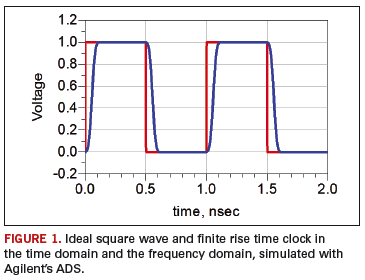
A very important waveform in the time domain and the frequency domain, to which most other waveforms are compared, is an ideal square wave. In the time domain, an ideal square wave has a zero psec rise time and a 50% duty cycle.
Its spectrum has three important features:
Only multiples of the fundamental appear.
The harmonic of each component drops off like 1/n, the harmonic number.
The even harmonics, i.e., 2d, 4th, 6th, etc., have zero amplitude.
For an ideal square wave, the frequency components continue with their pattern to infinite frequency, always dropping off inversely with frequency or harmonic number. But, if the rise time is finite, this is not the case. After some frequency, which we call the bandwidth, the amplitudes of the frequency components drop off much more quickly than 1/f for an ideal square wave.
Figure 1 shows a 1 GHz ideal clock square wave spectrum and the spectrum of a clock with a rise time that is 5% the clock period. The relationship between the 10-90 rise time, RT, and the bandwidth, BW, is roughly approximated as BW = 0.35/RT. For this example, we would expect the bandwidth to be about 0.35/0.05 = 7 GHz. This is about where the amplitude begins to drop off below the ideal square wave spectrum.
Every frequency component of an ideal square wave is significant in contributing to that 0 psec rise time. However small the amplitude may be at very high frequency, it is still important. Remove any and you won’t get the 0 psec rise time.
When the frequency component of a real waveform has an amplitude significantly smaller than the equivalent ideal square wave, it won’t be large enough to contribute to the rise time and can be ignored. The bandwidth of a real waveform is the highest sine wave frequency component that is significant. Decrease its bandwidth in the frequency and its rise time in the time domain will increase.
A fundamental measure of the rise time of a signal in the time domain is the frequency at which the harmonics begin to drop off more quickly than 1/f. For this reason, the bandwidth is often referred to as the knee frequency. The lower the knee frequency in the frequency-domain, the longer the rise time of the signal in the time-domain.
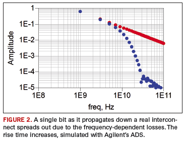
Signal propagation on real interconnects. How do real interconnects like traces on a circuit board, or coax or twin-ax cables, affect signals? In the time domain, we can evaluate the behavior of a single bit as it propagates down a transmission line. Figure 2 shows what a single 1 bit would look like traveling down a 0.003˝ wide FR-4 transmission line for a 1 Gbps signal, initially, after 30˝ and after 60˝.
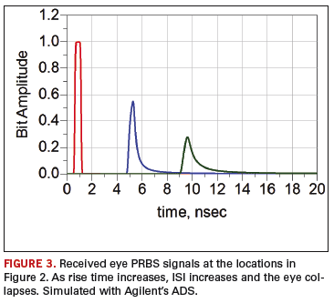
The single 1 bit starts out with a 1 nsec unit interval, and a very fast rise time. As it propagates down the transmission line, the wave form is dramatically affected. That single bit spreads out into adjoining bits. This cross talk between one bit and other bits is called inter-symbol interference or ISI. It contributes to the collapse of the eye. Figure 3 shows the received eye of a pseudo random bit stream (PRBS) signal at the three locations above.
How the single bit spreads out is a very important metric of the behavior of the interconnect. Yet, as viewed in the time domain, the exact shape of the pulse is complicated and difficult to describe in a simple way.
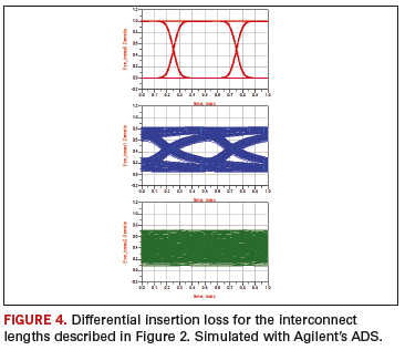
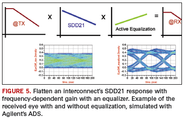
Here is where the frequency domain description offers a simpler description. The term that describes how a sine wave differential signal is affected by an interconnect when it exits is the differential insertion loss, sometimes referred to by its S-parameter designation, SDD21. This is also called the transfer function of the interconnect. This measureable property describes what a sine wave with amplitude of 1 looks like when it comes out the transmission line. The differential insertion loss for these interconnect paths is shown in Figure 4.
Every single interconnect has a similar SDD21 response. The amplitude coming out is always less than the amplitude going in, and the amplitude of SDD21 drops off with increasing frequency. On a log scale of amplitude, measured in dB, the differential insertion loss generally drops off nearly linearly with frequency. A metric of the dB/inch per GHz is one single number that characterizes most interconnects.
If we send an ideal square wave signal into a real interconnect, its spectrum will be multiplied by this transfer function. The SDD21 tells us how each frequency component will be attenuated. Higher frequencies get attenuated more than lower frequencies. This pushes the knee frequency of the signal’s spectrum to lower frequency, and increases the rise time of the signal.
This frequency-dependent attenuation of typical interconnects will cause rise time degradation, which will smear one bit into adjacent bits, result in ISI and cause collapse of the eye.
It’s not the attenuation of the interconnect that degrades the rise time; it is the frequency dependence of the attenuation. After all, if we take all the frequency components and just attenuate each of them the same amount, we will still have the same spectral shape of the bit sequence coming out. The frequency at which the knee occurs will be unchanged; the rise time of the signal will be unchanged, and there will be no ISI and no collapse of the eye.
Fixing the eye collapse in the frequency domain. We can fix the ISI in real interconnects by either flattening the insertion loss curve of the interconnect, or by changing the spectrum of the signal going into the interconnect so that when it comes out, it preserves the 1/f shape.
Designing an interconnect with a flatter response is tough. The root cause of the frequency-dependent loss is the combination of the skin depth dominated copper series resistance and the laminate material dielectric loss. For example, certain Gore cable assemblies use a very thin signal conductor, which has a frequency-dependent resistance much flatter than a typical copper core cable.
Likewise, laminates such as Rogers’ RO4350 have a lower dissipation factor and a flatter response dielectric loss curve. Both these interconnect design features reduce ISI with a flatter differential insertion loss response.
It is also possible to flatten an interconnect’s transfer function by adding some extra frequency-dependent gain at the receiver. If the interconnect has more attenuation at higher frequency, why not add gain that increases at higher frequency to compensate and flatten the overall response? Figure 5 shows how this works.
When we add frequency-dependent gain, we equalize the response of the interconnect across a wide frequency range. We call this process equalization. The ideal equalizer has a gain curve that is the exact inverse of the attenuation curve. With a flat response, the spectrum of the transmitter is preserved at the receiver; the knee frequency is the same as the transmitter; the rise time is the same, no additional ISI and no additional collapse of the eye.
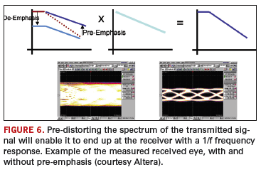
Finally, the spectrum of the signal at the transmitter can be pre-distorted to add extra high-frequency components. The interconnect will attenuate the high-frequency components anyway. If we add extra high-frequency components at the transmitter, by the time they travel through the interconnect, they will be attenuated away, leaving the 1/f spectrum of a short rise time signal. The shorter the rise time, the less the ISI, and the lower the eye collapse.
One way of implementing adding high-frequency components is called pre-emphasis. Wherever a 1 bit begins, extra energy is added. Likewise, we could obtain the same pre-distorted spectrum by taking out low-frequency amplitudes. Whenever there is a string of more than one bit with the same value, reduce the signal level. This is called de-emphasis (Figure 6).
Both pre- and de-emphasis result in the same distorted shape in the transmitted signal spectrum. When either of these distorted signals travel through an interconnect, if optimized for the interconnect, the signal will come out the other end with a short rise time, less ISI and a more open eye.
By looking in the frequency domain, we can see how the techniques mentioned manipulate the frequency domain spectrum of the received signal. We engineer it to look more like an ideal square wave’s spectrum and recreate the shortest rise time to minimize its ISI and keep the eye open so that each bit can be detected as its true 0 or 1 value.
Even though final performance is always measured in the time domain, sometimes detouring through the frequency domain may be a faster route to a signal integrity solution.
Au: Many of the principles described in this paper are covered in great detail in papers that can be downloaded from bethesignal.com.
Eric Bogatin, Ph.D., is a signal integrity evangelist with Bogatin Enterprises (bethesignal.com); This email address is being protected from spambots. You need JavaScript enabled to view it..


 I heard recently that another friend and printed circuit board designer who works for a company primarily known for producing large industrial and farm equipment will soon be out of a job. Yes, like many before them, the company is moving the circuit board design department offshore, in this case, to India.