Labor and manufacturing processes will be severely reduced, but daunting barriers remain.
Many electronics industry veterans have heard about, but have limited understanding of, a breed of materials science called printed electronics. This field involves thin films, coatings and inks that perform electrical functions (conducting, semiconducting, insulating, etc.) similar to silicon electronics, with one exception: They are applied in a continuous and often soluble process across a variety of substrates (glass, paper, flexible and special polymers, etc.), as opposed to via a rigid and brittle silicon deposition process that yields products in batch and on a massive scale.
Why would such a technology represent a threat to a sector that has grown to be over a trillion dollars in size? The answer seems to be in the upside potential that printed electronics represents that concern printable (that is, configurable-on-demand) electronics circuits with integral qualities and capabilities involving multiple components such as sensors, amplifiers, antennas, battery, audio, display and wireless communications that today are manufactured and assembled as discrete components.
To appreciate printed electronics’ potential, it’s important to understand how it works technically. Consider traditional printing processes: flexography, gravure, inkjet, offset printing, screen printing, and thermal transfer. It is clear these methods have been developed to solve unique printing applications (newspapers, magazines, business documents, various other forms of mass printing), yet they also can be applied in electronics if the correct materials (organic and inorganic) can be produced to perform electrically functional applications. It turns out, this is what’s happening.
Printed electronic products are printable at different levels of resolution, conductivity (material blends), layers, sensitivity, size and speed. This can vary according to the particular kind of print technology being used: continuous, high-speed throughput, wide format, or simply low cost. As such, new products are being engendered that work outside the current paradigm of semiconductor and circuit board technology.
New Organic Electronics Organic conductors are lighter, more flexible and less expensive than inorganic conductors. This makes them a desirable alternative in many applications, provided high performance is not essential. (While conductive, they are not as fast or efficient as inorganic materials such as silicon or copper.) But this difference creates the possibility of new applications, such as electronic paper or smart/flexible windows, which would be impossible using traditional technologies. Additionally, organic conductive polymers are expected to play an important role in the emerging science of molecular computing.
Until now, circuits built with organic materials have permitted only one type of charge to move through them. The latest research provides for charges that flow both ways by positive and negative charges. Over the past 30 years, researchers have been working to make organic electronics by layering two complicated patterns on top of one another: one that transports electrons and another that transports the positive holes. Recently, polymers have been created with a donor and an acceptor part that can transport both positive and negative charges in one material. The material would permit organic transistors and other information-processing devices to be built more simply, in a way that is more similar to how inorganic circuits are now made.
Yet, printed materials and conductive inks have begun to penetrate many established products and extend them in new ways. Kovio was the first company to make an entirely printed transistor-based RFID device with nanosilicon on stainless steel foil, and PolyIC on its website is promising kits of transistor RFID in 2010. To this end, antennae have been printed on certain RFID tags by companies such as Hyan Label (China), which can print directly on paper adhesive labels using reel-to-reel transfer.The number of transistors on these tags is small, therefore so is the performance, but potentially the cost is low if done in volume.
The primary goal of making organic transistors and integrated devices is to create circuits that are functional, inexpensive and printable on-demand. Organic thin-film circuits can take the place of silicon circuits in applications that require short turnaround times, flexibility and configurable performance. Moreover, organic materials can be rendered into a liquid form and applied at room temperature and atmospheric pressure, and thus are ideal for printable formats. Thus, this emerging breed of low-cost electronics can easily and quickly be applied via conventional ink-jet technologies at minimal cost.
By combining different print and production techniques, these polymer electronics can be engineered in conductor paths of any desired length, with print layers of 1/1,000 mm thick. As the process technology evolves, polymer electronics will be able to integrate hybrid designs so that transistors, diodes, memory, and displays can be provided in a continuous and mass-printed form. To date, polymer electronics have produced touch-sensitive sensors (keys), digital memory (16 to 96 bits, depending on the available surface area on the substrate), processor logic, photovoltaic batteries and color displays. Yet printable inorganic materials and composites are being developed that form a class of conductors with vastly better conductance and cost, ideal for producing superior printed laminar batteries, large electrophoretic, electroluminescent and electrochromic displays and solar cells. Moreover, inorganic materials have been applied to quantum dot devices and for transistor semiconductors such as logic and memory (zinc oxide) devices with 10 times the frequency and mobility of organic devices, in addition to greater stability.
Composites include oxides, amorphous mixtures and alloys. Increasingly, organic devices such as OLEDs employ a variety of inorganic materials such as boron, aluminum, titanium oxides and nitrides as barrier layers against water and oxygen. Similarly, aluminum, copper, silver and indium tin oxide are used as conductors, while calcium or magnesium can be developed as cathodes, cobalt-iron as nanodots, and iridium and europium in light-emitting layers on displays.
In 2009, inorganic semiconductors were being sold by companies such as Kovio for RFID tags due to much higher mobilities versus what is found in organic semiconductors. Similarly, companies such as Pelikon and elumin8 have applied inorganic materials to flexible electroluminescent displays that involve six to eight layers, including a copper-doped phosphor. These displays can be deposited on plastic or other film substrates that can cover meters of square area and are capable of emitting a range of colors.
Labor Reduction Printed electronic circuits eliminate the required traditional subtractive wet process used today, which includes etching, stripping, metallization and copper plating. Without the costly process finishing, significant savings occur in labor, equipment and water consumption. These savings are further extended by way of wastewater treatment and sewer user fees, which involve the use of formaldehyde, chelators, ammonia, heavy metals and acids. Electric and gas consumptions see a notable reduction by eliminating the need to heat most of the wet processes, multilayer presses, and the large plant-wide demand for compressed air. HVAC reductions also are experienced due to greatly reduced exhaust requirements.
With the reduced amount of the many complex chemical processes to monitor, high overhead labor is eliminated. Printed electronic circuits (PEC) are expected to use 20% of the current labor requirement with the same square foot output. A printed circuit line of conductive silver and ceramic dielectric inks allows for a circuit to nearly equal the resistance properties of etched copper by controlling both the thickness and the width of the conductor, and therefore the overall resistance of the trace. Moreover, PEC permits the interconnection to be accomplished using highly conductive nano-inks without the need to drill holes or solder components. By eliminating the drilled via hole, printed circuits increase the interconnect reliability because the vias are 100% filled with silver ink and have equal resistance to a drilled plated via.
The special conductive inks permit a drilled hole to be filled with silver and re-drilled smaller to create a very strong conductive through-hole, if desired.
PEC gets particularly interesting when considering flexible surfaces or when active functions are required such as contamination detection or time/date sensitivity. Adidas, for example, has striking innovations involving smart clothing and fabrics that measure body data to help better manage health or achieve optimal athletic performance. The application that has made the most inroads in PEC can be found in “plastic” electronics, in which carbon compounds have created a new class of electrophoretic display used in today’s popular e-readers, such as the Kindle and Nook. Organic light-emitting diodes (OLEDs) can now be printed on a variety of flexible surfaces and open new applications in displays, signage and packaging.
Printed electronics will emerge in some of the most mundane and unobvious sectors. For example, PEC will have an enormous impact on the consumer sector, giving products special appeal by combining unique displays and signs, producing sounds and information on a product’s packaging. Cosmetics that rely on color shapes will be enhanced with unique lighting and audio features on the display shelf. Another application is foods or pharmaceutical packages that are time-sensitive for freshness, safety and potency, not to mention detection monitoring for toxins or efficacy. Perhaps more exciting, printed electronics is a precursor to many nanotechnology innovations, including engineering bionic limbs that integrate carbon nanotubes with human nerves, and artificial implanted hairs that detect pressure/temperature sensing, yet are dispersed in a flexible polymer composite skin. This stuff is now emerging and preeminent.
Barriers to Growth The market for printed electronics has become reality, albeit not at the rate that many have predicted. The barrier to exponential growth seems to be the inability of suppliers to lower costs so that mass production can be adopted and demand generated. This is the classical economic dilemma with disruptive technologies when highly competitive and traditional alternatives exist that continue to innovate at similar rates and thus are difficult to displace.
NVR is now completing its second edition of its syndicated market research report titled The Worldwide Printed Electronics Market. This study looks at this technology, what it replaces and the opportunities it presents, but also the challenges that printed electronics faces. The results are disruptive, to say the least, and while the market potential is profound, just when and how is this expected to emerge? It turns out there are significant barriers to printed electronics’ ascendancy in the near future.
In the near future, printed applications concerning RFID and OLED displays will come, manufactured using OTFT (organic thin film transistor) technology. These technologies are penetrating a wide number of products, but not at the rate nor with the impact to displace traditional technologies. As costs decline and performance improves, customers will be justified to switch, and in many cases, entirely new design solutions will be created. For example, photovoltaic thin films are beginning to emerge along with battery storage technologies that could soon exceed the electrical efficiency of competing technologies and at lower costs. However, these solutions often involve tradeoffs such as a greater area to produce the same cost per watt, and so cannot be ubiquitous. Table 1 summarizes the worldwide market for printed electronics by product application in 2009.
Over the next 10 years, printed electronics will have direct impact in the RFID market, where low-cost printed tags with embed codes and biometric data can displace traditional barcode products by integral wireless technology in active devices. The implications are profound, including embedding ID information in passports, smart cards, transportation and freight, healthcare, manufacturing, prisons and agricultural tracking devices. Printable OLED displays will compete with tradition TFT devices in the areas of sub-displays, mobile phones, cameras, video, car audio and games where configuration, form-factor and power consumption are determining issues. Finally, printed PV thin films will gradually replace traditional poly-silicon technologies that so dominate the solar panel market today. Table 2 summarizes the worldwide market for printed electronics by product application in 2019.
The critical business distinction for printed electronics becomes one of scale, volume and cost/performance, whereby printed electronics will often be at a disadvantage to traditional electronics. Yet we have seen disruptions such as the demise of CRT televisions by more expensive flat screen TVs because of better performance and functionality. Why should printed electronics not displace certain semiconductor logic and memory components that integrate transistor circuits with display, antenna and audio technology in a single device?
The nexus lies in the R&D investment that exists within the semiconductor and flat panel industry that vastly exceeds any being made by printed electronics. Yet much of the breakthrough work is borne out of the national labs, government research agencies and corporate R&D departments, among such companies as 3M, Applied Materials, Fujitsu, HP, Intel, Samgsung, Sharp, Xerox and a host of more exciting lesser-knowns such as E-Ink, elumin8, Kovio, Nanoink, Plastic Logic, PolyIC, T-Ink, and Thin Film Electronics. These companies are incrementally producing breakthrough technologies that potentially will be the cornerstones of paradigm-shifting products that could make parts of the semiconductor industry obsolete and noncompetitive.
We live in a time when innovation is constantly evolving. While it is always difficult to predict the growth curve for disruptive technology, printed electronics stands to take the electronics industry in a new direction. What better time is there for those on the cutting-edge to make their value-proposition fresh and compelling? We look forward to monitoring these new innovations and measuring their cross-impact over the next several years. CA
Randall Sherman is president and CEO of New Venture Research Corp. (newventureresearch.com); This email address is being protected from spambots. You need JavaScript enabled to view it..
Several devices perform well under vibration and temperature cycling testing.
We recently characterized the reliability of surface mount RF components. The RF frequency band of interest was the X band (10.7 to 11.7 GHz). A two-pronged test for printed circuit assembly reliability was designed for both extreme thermal cycling and vibration. The rapid thermal cycling and extreme vibration testing simulates the total stress encountered by the assembly over the life of the product, but accomplishes it in a relatively short period of time. To perform the reliability testing, a test vehicle consisting of a printed circuit board with test structures and components was designed, fabricated and assembled onsite.
The surface mount technology components selected were commonly used and have operating ranges up to the X band of the RF spectrum. A digital attenuator in a quad flatpack, no-lead (QFN) package was used with supporting chip components in 0402 and 0603 sizes. Two surface mount hybrid couplers with different leads were installed: one with L leads and one with castellated leads. Side launch SMA connectors with through-hole ground connections were installed to permit connection to the spectrum analyzer.
The frequency range of the attenuator is up to 13 GHz, while the other RF components are less than 4 GHz, based on their application in the actual circuit. The test vehicle was designed to simulate a proposed board stackup and permit the mounting of the SMT RF components. Each board has six RF paths that pass through the components (Figure 1). To observe any effects of vibration and thermal cycling on the laminated board, three RF paths were designed with no components to act as controls.
Component manufacturer’s data sheets were used to define the shapes and sizes of both the pads on the CCA and the cutouts for the solder paste stencil. The stencil thickness was 0.005˝ to permit the proper solder volume on the 0402 and 0603 component ends. The larger, castellated lead coupler required a stencil with a “window pane” feature to reduce the volume of solder used to solder the large center ground to the ground plane.
The solder paste selected was the type typically used for military assemblies (SnPb37 with a no-clean flux and a J-STD-004 classification of ROL0). The board layout was programmed into a pick-and-place machine so the QFN and 0402 components could be placed accurately. A double-reflow process was used. All flux residue was removed using an inline cleaner to meet IPC-A-610 Class 3 requirements.
Accelerated testing plans. Component reliability was tested using accelerated temperature cycling based on JEDEC Standard JESD22-A104. The assemblies cycled between +85°C to -40°C for 1,000 cycles of 91 min. each. Breaks for RF testing occurred at 100, 200, 400 and 1,000 cycles to permit more resolution into the possibility of early thermal failures.
Vibration testing also was performed to simulate the stresses of motion on the components over the assembly’s life. The three axes vibration testing was performed for two hours at frequencies from 4Hz to 50Hz per MIL-STD-167 Type 1. The test vehicles were RF tested prior to being sent for vibration and then RF tested again on their return to the EMPF.
Thirty test vehicles were assembled using in-house SMT equipment. Prior to thermal cycling and vibration testing, each of the RF paths on all the assemblies was visually inspected and swept for transmission loss (S21) and insertion loss (S11) to gather baseline data. An Anritsu Spectrum Analyzer was used and data were gathered from 40 MHz to 20 GHz.
Fifteen CCAs were sent for thermal cycling and 15 were sent for vibration testing. After vibration testing, there was no evidence of cracked solder joints or other evidence of stresses between the devices and the board. The RF paths on each of the 15 assemblies were swept, and data showed no significant degradation in the device or path performance (Figure 2).
Fifteen CCAs were run through 1,000 thermal cycles with visual inspection and RF testing performed at established break points. Again, no evidence of damage was apparent on the visual inspections, and no significant degradation in performance was apparent on any of the CCAs after RF testing (Figure 3).
The analysis showed no significant degradation of performance. Visual inspection of the components and solder joints showed no physical damage and almost no degradation in performance through the accelerated life tests (Figures 2 and 3). Although the figures shown are for one specific device through the tests, all other SMT components performed as well. CA
ACI Technologies Inc. (aciusa.org) is the National Center of Excellence in Electronics Manufacturing, specializing in manufacturing services, IPC standards and manufacturing training, failure analysis and other analytical services. This column appears monthly.
A trying year was dramatized by two unfolding stories: the economy and Elcoteq.
When it comes time to write the story of the EMS industry in 2009, foremost will be the effects of the recession. There is another story, however: the dramatic fall of Elcoteq, the former cellphone wonder whose sales have rollercoastered from a high of 4.28 billion euros (about $6.17 billion at today’s conversion rates) to an estimated 1.54 billion euros ($2.2 billion) at the end of 2009.
Last year felt in many ways like the nightmare of 2001-02 all over again. Factory shutdowns among Tier 1 and II EMS companies were the norm, with Flextronics, Celestica, Sanmina-SCI, Plexus, Benchmark, Jabil and Elcoteq all cutting plants and people. Most of the closures came in Europe or the US, where even mighty Foxconn shuttered a 400,000 sq. ft. PC assembly and enclosures plant in Fullerton, CA, relocating or letting go some 600 workers. (Most but not all: Flextronics, for example, shuttered its factory in Kuala Lumpur, the former Casio Computer site it acquired in 2002.) The differences between last year and the tech recession of 2001 were telling, however, in that EMS companies this time around acted with accordance with clear and aggressive strategies. It was as if, after the last go-around, the majors decided that if and when another industry recession hit, they were not going to react passively.
Key moves during the year include Asustek’s decision at year-end to split off its Pegatron manufacturing group, creating overnight one of the world’s largest ODM companies, and Venture’s decision late in the year to push harder into ODM work, which many see as more profitable than traditional EMS services. But while analysts and pundits continue to predict (guess?) that one or more of the top-tier EMS companies would be bought or closed, all – with the notable exception of one (see sidebar) – appear to have learned from past mistakes. They kept their inventories in line, their balance sheets clean, hoarded cash and refinanced near-term debt in order to ensure survival. They also cut fast and deep.
Almost every major EMS company saw revenues fall last year. For most companies, the first or second quarter was the trough, and sequential gains were seen through the rest of the year. In all probability, a return to 2008’s revenues will be a few years away. Among the top 20 companies, No. 1 Foxconn was an exception – barely – with sales growing less than 1%. Another outlier, No. 7 Cal-Comp Electronics, actually grew year-over-year the first two quarters, then fell behind by 8% year-over-year during the third, despite turning in its best revenue period of the calendar year. No. 13 Beyonics, Singapore’s largest EMS company, was up big and will be banging on the door of the Top 10 if it can keep up the pace.
With no major acquisitions or mergers during the year, there were few big changes to theCircuits Assembly Top 50 list. Falling off this year’s Circuits Assembly Top 50 is one company that, in hindsight, never belonged. Viasystems, which is relisting its shares, and as such began to break out its revenues, was in retrospect nowhere near the $504 million in sales we estimated last year. Hitachi Computer Products America announced in late fall it would exit the electronics manufacturing services business (albeit much of its EMS work was likely for its parent company). The biggest shock, however, was Jurong Hi-Tech, which came in at 26th last year. The Singaporean EMS company imploded under accounting irregularities and sold off its assets. (Needless to say, it did not make this year’s list.) And our apologies to Team Precision, Eolane, EPIQ and Electronic Network, all of which should have made last year’s rankings.
Besides Jurong, the two companies that appeared hardest hit in 2009 were Elcoteq and Surface Mount Technology (Holdings) Ltd. The former took a body blow from Nokia, which pulled all its assembly work in-house, taking an estimated $5 billion worth of EMS work offline. As a result, the company’s revenues fell more than 50% last year. Unlike Elcoteq, whose fate is heavily tied to the telecom and handheld sectors, Hong Kong’s SMT Holdings operates in more balanced markets. The company’s revenue comes primarily from industrial controls, computer peripherals, consumer and automotive, each of which makes up 15 to 35% of the firm’s revenues. Since the company does not disclose its major customers, it’s hard to discern why its sales drop (roughly 45%) was decidedly worse than the industry average.
What is always interesting about tallying up the revenues of EMS companies is how inflated the sums are. Macroeconomists might disagree with me, but the amount of double-, triple- and quadruple-counting is staggering. The rule of thumb is about 80% of the assembly’s cost is for materials, and most EMS companies no longer buy on consignment, which means the value of single chip gets highly distorted as it makes its way through the supply chain.
Take your average PC. Intel makes the microprocessor and sells it for $250 to Foxconn. Foxconn builds the board and box and ships it to Dell. Dell sells the finished PC to the customer. Each company adds that $250 (or whatever markup it uses) to its revenues, which means that original chip has now accounted for $750 worth of sales. Throw in a retailer like Best Buy, and perhaps a distributor like Arrow and now that same chip is worth $1,250 in accounting terms by the time it reaches your desk. In doing so, the size of the industry becomes highly inflated. Not that the same scenario doesn’t play out in just about every sector imaginable, but it is something to keep in mind when considering the “real” size of “S” (services) in EMS.
To sum up 2009, we learned that putting all your eggs in the basket of a consumer electronics customer could reap great dividends, or great hardships. Whether Elcoteq can return to glory or slips further into the abyss will likely be the story of 2010 too. CA
[Sidebar] Elcoteq’s Miserable Year
No company took it on the chin worse last year than Elcoteq. Sales plunged about 55% year-over-year to an estimated 1,537 euros ($2.46 billion) and are now about 65% off their 2006 high. Global headcount was reduced about 50%, to 10,770. Factories in the US, Russia and China were either mothballed or shuttered. As if the economy itself wasn’t bad enough, its once largest customer, Nokia, pulled all its assembly in-house. As the year drew to a close, Elcoteq was scrambling to finalize a deal with Videocon to invest a reported 50 million euros to help shore up its balance sheet.
Circuits Assembly spoke with Elcoteq director, sales and product marketing Petra Ebner in November. Excerpts:
CA: You are in talks with Videocon to invest. What would this mean for Elcoteq?
PE: Videocon is a potential investor. We are currently in due diligence. The scheduled closing is year-end. It is not clear how this will look once a deal is done, but we’re not talking about them taking over. Elcoteq also is in talks with Kaifa [its largest shareholder].
We also have set certain goals: 1) Find an investor to increase our capitalization; 2) restructure debt – we are offering 15% of the dollar to our unsecured creditors; and 3) focus on more bottom-line customers. We are extending the market scope to higher-tech customers. Those end-products would be filters, RFID, industrial – companies that can benefit from our experience in communications.
CA: When your restructuring is finished, what will Elcoteq look like?
PE: We are now more focused on consumer electronics and systems solutions. We now have two factories in China; we closed Shenzhen. We have plants in Bangalore; Pécs, Hungary; Tallinn, Estonia; Monterrey, Mexico; Brazil. Russia has been mothballed. Pécs is the largest, with about 3,500 staff.
CA: Nokia decided to pull its assembly operations in-house. Any change in its plans?
PE: There are no signs from Nokia of business coming back.
CA: Given the product mix and choice of locations, it almost seems Foxconn has put a bulls-eye on Elcoteq’s back.
PE: Competing with Foxconn is a mission impossible. Customers are under so much cost pressure. Our focus is now the top line, not the bottom line. We want to grow with our existing customers, but we also want to see some different customers. Our focus is on lower volume and higher mix. When I came to Elcoteq, we had communications and industrial customers. I think we will return to that: more mid-sized customers; more box-build and tested finished product. Our target customer is $5 million to $10 million [in annual services provided].
CA: High-mix lines typically use different platforms than high-volume lines. Will your capitalization issues constrict your ability to invest in the right machines?
PE: We won’t need new equipment. In many cases, customers have supplied [it] as consigned equipment. We work with partners on plastics, etc.
CA: Is there an EMS company that Elcoteq is modeling its new strategy after?
PE: We haven’t picked anyone as a model.
CA: Is Elcoteq targeting alternative energy as a possible market?
PE: It’s not off our radar, but we are not thinking much about it. We are discussing with some solar companies about the equipment behind the panels – inverters, electronics, etc.
Mike Buetow is editor-in-chief of Circuits Assembly (circuitsassembly.com); This email address is being protected from spambots. You need JavaScript enabled to view it..
SI rules must take into account signal quality, timing and crosstalk.
Today’s high-speed busses, such as PCI-Express, DDR2/3, and serial ATA, running at frequencies from several hundred megahertz to beyond a gigahertz, make for tight timing margins. The fine-geometry silicon required for these speeds makes for very fast edge rates. And pressure for smaller and cheaper products makes for very dense PCB layouts. All these factors necessitate high-speed analysis, and the subsequent generation of routing constraints, to implement a successful high-speed printed circuit board design.
There are three main areas of concern when developing high-speed design constraints: signal quality, timing, and crosstalk. When taken together, these three factors can be called signal integrity (SI) constraints. Defining the constraints for each of these forms a set of SI rules, under which the design must be executed.
Signal quality includes items like overshoot, ringback and non-monotonicities: items that can damage a receiver or introduce data errors. Timing at the PCB level, including effects of terminations, receiver loading, and trace impedances and lengths, must be rigorously analyzed to ensure compliance at the system level. Crosstalk, which is unwanted noise induced by one trace onto another, can affect both signal quality and timing. Ensuring proper system operation requires all these analyses. The resulting constraints drive trace lengths, topology and spacing. This, in turn, drives items like parts placement. It is also necessary to constrain items like board stackup, trace widths, and copper weights. Clearly, high-speed PCB designs should not begin without the proper analysis.
Signal quality. Digital logic reduces data to a series of 1s and 0s, which are represented in a real system by high and low voltages. A receiver discerns whether a voltage represents a 1 or a 0 when that voltage is above or below the logic thresholds of the receiver. Also, that voltage must not exceed the limits (upper or lower) of the receiver, or it might be damaged. These two requirements generate two fundamental constraints in signal quality analysis: ringback and overshoot.
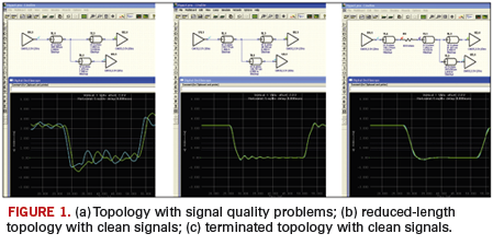
If a designer were to just connect a transmitter to two receivers, the result would be something like the waveform in Figure 1a. Here, ringback and overshoot violations can be seen. The green waveform, which is the receiver in the upper right of the topology, shows negative overshoot in excess of 1.4V (magnitude). The blue waveform, the other receiver, rings back to 0.8V, which is the lower logic threshold. If a PCB were built with this topology as is, errors in the data stream would occur, and the receivers could be damaged.
If the topology lengths are reduced significantly, to well below the length of the signal edges, these receiver waveforms get cleaned quite a bit (Figure 1b). Unfortunately, however, such lengths are typically on the order of an inch or so, which is not always feasible in a design.
Another method of cleaning the signal at the receiver is to use termination impedance. Termination matches the impedance of the drivers and receivers to the board traces, controlling the reflections that create overshoot and ringback violations. Using termination also permits much greater flexibility in the lengths of various parts of the topology. The trace lengths aren’t restricted to an unrealistic maximum, while still permitting clean signals.
Termination values may be taken from bus design guidelines, but in the absence of such guidelines, can be determined from analysis. Some tools determine the values for a termination automatically by looking at the topology. Beyond that, the location of the terminator within the trace topology can be determined by varying those lengths and analyzing the results. Maximum length rules for determining where the terminators may be placed are created from this analysis, as well as length constraints for the other traces in the topology (Figure 1c). All these lengths may be explored to create the widest solution space for the layout designer, which still meets the signal quality requirements.
Timing. Most length constraints in a design come about from a timing requirement. Timing requirements come from the fact that data are “clocked in” to a receiver at certain intervals. If the data are not there when the system needs them to be, it won’t work. There are two main types of bus timing architectures – common clock and source synchronous – that lead to two types of layout constraints: min./max. and matched lengths.
Minimum and maximum delay constraints are created from common-clock bus architectures. An example of this would be PCI, where data are clocked out of a transmitter and into a receiver using a common clock. To make sure the data are not there early, or violate the hold time requirement, a minimum length constraint must be created. To ensure the data do not arrive too late, a maximum length constraint is created. These constraints are not merely based on the length of the line, however. Many other considerations such as receiver loading and signal quality issues determine when the transmitted data may be valid at the receiver, so proper signal analysis must be performed to calculate these lengths appropriately.
Matched delay constraints come about from source-synchronous busses. These busses, such as DDR2, send a clocking signal or “strobe” along with the data to clock it in at the receiver. This eliminates the complex timing relationship between driver and receiver, and requires only the matching of the strobe to the data. Typically these interfaces have other concerns, such as signal quality, which determine when the data are valid. The main timing constraint for these busses is the matched delay constraint, which becomes tighter with increases in bus speed or signal quality problems.
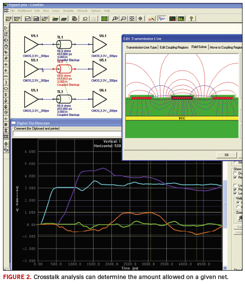
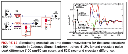
Crosstalk. Another important constraint for the layout is the spacing between traces. The spacing limit is determined by the amount of crosstalk that occurs between the signals. A number of factors influence crosstalk: the edge rate of the driver, the board layer stackup, the amount of parallelism between traces, and, of course, the spacing between traces. Crosstalk affects both signal quality and timing, and the amount of crosstalk allowed on a given net can be determined from simulation. An example of a crosstalk simulation is shown in Figure 2.
Crosstalk analysis typically consists of a “victim” trace and two “aggressor” traces. More aggressors can be included, but in most cases, 95% of the crosstalk will come from the nearest two. With models for the driver and receiver, as well as the board stackup built into the simulation, the spacing between the traces can be modified to determine an acceptable level of crosstalk. The length the traces run parallel also can be modified to view the effects. The main result of such an analysis is a spacing rule between traces. If that spacing rule could not be met, or if greater flexibility is to be permitted in the layout, a rule could be created with tighter spacing, but also with a maximum parallelism constraint. Such a pair of constraints could be created from crosstalk analysis, and modified as demands change.
Multi-gigabit/SERDES analysis. The same concerns of signal quality are at the forefront of analysis for SERDES busses such as PCI-Express and serial ATA. These busses do not have the same delay constraint as traditional, parallel busses, since they do not have an external clock. Most delay constraints associated with these kinds of busses are to match the two sides of the differential signal very closely. Because multi-gigabit signals use differential signaling, and have rise/fall times less than 100 ps, it is important to match both sides of the differential signal to less than 10 ps, which translates to a length of just tens of mils on a PCB. Crosstalk is also a concern on these busses, especially since they operate at lower voltages than 3.3V and 5V logic, and therefore are more susceptible to crosstalk from those signals. Crosstalk analysis is done on SERDES busses much as it is on other busses, and spacing from other signals will typically need to be much larger than is typical.
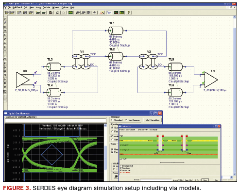
The biggest threat to multi-gigabit signals is loss. As frequencies increase, so do the loss effects. The biggest contributor to loss is length, which is why there are typically maximum length constraints on SERDES busses. Loss is also affected by the dielectric material used in the board, as well as the width of the traces carrying the signals. Other pieces of the signal path, such as vias, can also adversely affect the signals. All these effects are included in an appropriate eye diagram analysis, which gives a comprehensive view of the worst-case signals transmitted on the bus (Figure 3).
The results of such a SERDES analysis include maximum length constraints, trace width and spacing requirements, as well as layer constraints. Being able to explore changes in these items, such as modifying via geometries and layer changes, is vital to ensuring success in a SERDES design, while maximizing routability and flexibility in the layout.
Post-route verification. Once you have created all the necessary routing constraints for your design, and routed the board using those constraints, it is useful to verify that the board meets the original electrical requirements that prompted those constraints. Post-route signal analysis on all nets of a board is a good way to close this loop. Post-route analysis is an excellent complement to the rigorous pre-route or “what-if” analysis performed earlier in the design cycle. It is another step in the series of tasks performed to analyze high-speed busses.
Signal integrity analysis and verification is critical with high-speed designs. Signal integrity – signal quality, timing, and crosstalk – can result in data loss, errors, non-functioning circuitry, and even component damage if not controlled with a set of rules or constraints. Worse, many of these errors are highly intermittent, making them extremely difficult to fix after the fact, and component damage can be cumulative, meaning failures occur “down the road.” Without these types of analyses, and the constraints created as results, modern digital systems could not be designed to meet the cost, size, and performance needs of today. PCD&F
Patrick Carrier is a technical marketing engineer for high-speed PCB analysis tools at Mentor Graphics (mentor.com); This email address is being protected from spambots. You need JavaScript enabled to view it..
Higher signaling speeds require better signal integrity, thus designing multi-GHz or multi-Gb boards has to involve better knowledge and tools than ever.
Impedance measurements. Traditionally, impedance is measured by time domain reflectometry (TDR) on test coupons. Test coupons are manufactured on the same panels as the actual PCBs, and contain the same controlled-impedance traces (same width, same layer). Reason: It is easier to probe traces on a test coupon than on an actual, dense PCB.
TDR instruments generate a single very short pulse signal, and measure the reflected or arrived signal at the other end of the trace. Based on the TDR result voltage levels, the instrument or user performs some post-processing to get the measured impedance.
To take accurate frequency-dependent impedance measurements, set the TDR instrument to the same rise time as the signal would have on the actual PCB on the appropriate signal trace. (In practice, manufacturers don’t do this, although most TDR instruments have the option to set the rise time. Normally, a manufacturer has its favorite rise time setting and uses it for all measurements.) Some TDR instruments don’t have the option to set rise time; others do. This could lead to measuring impedance on a different frequency than it should be, and could result in a measurement error (Figure 8). The error is relative to the requirement, not an absolute value to the ideal impedance, since in reality, both the impedance requirement and the measurement are frequency-dependent.10
One way to do single frequency-point impedance measurement is to use a vector network analyzer (VNA) instead of a TDR. There are simple programs based on analytical equations, but they are outside of the scope of this article, as the calculation error can be 5 to 50%. Instead, we are focusing on field-solver programs, for which the only possible inaccuracies are the not-infinite mesh density, the wrong frequency, simplified modelling and improper usage. (For most programs, the software developers internally set mesh density.)
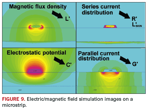
Field-solvers divide the geometry (2-D cross-section) into small pieces (nodes) – a process called meshing – and then solve the Maxwell’s differential equations in all of them to determine electrostatic and magnetic fields and current distribution (Figure 9).
Next, as post-processing on these fields and currents, they determine the RLGC per-unit-length parameters. Finally, they calculate impedance as described. Typically, they calculate w –> Z0 directly, and if the opposite way of calculation is needed, then they iterate until they reach the desired characteristic impedance within a user-specified tolerance (0.1 to 5%). Some samples:
Polar Instruments Si8000. This is the industry standard frequency-independent impedance calculator. It calculates everything on 2 GHz. The Dk value must be pre-compensated to the signal’s frequency or to a suitable value. (For computer boards, 2 GHz is sufficient.) It calculates both width –> impedance and impedance –> width.
Polar Instruments Si9000. This is the extended version of the Si8000, with some frequency-dependent parameter calculations. It only calculates width –> impedance in a frequency-dependent form, and impedance –> width only in a frequency-independent way, or with manual iterations. For the former, it compensates (as an option) for Dk over frequency.
Polar Instruments Speedstack. A stackup builder, it uses Si8000 or Si9000 for impedance calculations, but its material library does not support frequency-dependent Dk specifications. So, in case of using together with Si9000, we need to override Dk, impedance and width values.
TNT-MMTL (open source; available at Sourceforge). Developed by the Mayo Clinic Special Purpose Processor Development Group, it can do both ways w –> Z0, and w –> Z0. In comparison with the Polar Si8000 in a few different tests, I calculated a maximum 2% difference for coated microstrips, and less than 1% for stripline structures. This is frequency-independent.11
Appcad RLGC. This program calculates the transmission line RLGC parameters, and the user has to calculate the impedance from them. This is frequency-dependent.12
General-purpose 2-D field-solvers. Examples include Ansoft Q3D Extractor, FEMM (FiniteElementMagnetics, open source). These programs provide the opportunity to set every simulation parameter, so they can be used on any levels of accuracy. We can draw any arbitrary-shaped cross-sections, and model multiple material platings on the conductors. They only work in the width (geometry) –> impedance way. They are normally frequency-dependent. The simulation setup may take several hours, since we have to hand-draw the geometry, do mesh seeding at critical areas and specify material parameters, perform simulations, and post-processing. After several simulations, we can get the RLGC parameters or matrices to use to calculate impedance.13
Frequency-Dependent Impedance Control Drawbacks There are certain problems with frequency-dependent impedance control. For one, at the time of this writing, there was no available accurate, fast method/software to calculate trace width from impedance requirement on a user-specified frequency.
Second, PCB manufacturers do not perform frequency-dependent impedance measurements. They often say they do, but usually they have their choice of a specific signal rise time, yet it is fixed for all their measurements. The basic principles of TDR impedance measurements are frequency-independent. There is no method under which TDR could discern the test coupon impedance on a given frequency, since the TDR signal also is a wideband signal. One way could be to set the TDR test signal at a similar frequency spectrum as the digital signal, which – simplified – means setting the same rise time on the TDR as the digital signal. But it is not proven why it would be more accurate, and the theory remains under study.10
Third, there is no exact method found for time domain to frequency domain signal conversion. For digital signals, it is hard to select a single frequency, since they are wideband signals and defined in time domain. There could be several user-based choices (knee frequency, clock frequency, mean of band, etc.) to pick up as a part of the signal’s frequency spectrum. So, the selection leads to more inaccuracies.
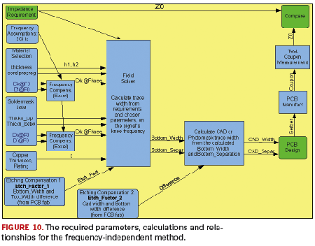
Frequency-Independent Impedance Control This is a subset of the previously described frequency-dependent method. On a certain level, it still must be frequency-dependent: As a minimum, we must compensate for the frequency dependence of the dielectric constant, since it usually is provided on a very low frequency (1 MHz). Before putting material Dk and Df information into the calculator or its library, compensate for them to a suitable frequency (e.g., for computer boards, 2 GHz is sufficient) (Figure 10).
The method is the same as described in the frequency-dependent calculation, with the following differences:
The field-solver does not need the Df data, but the Dk compensation still does.
The TDR measurements can be done with the usual constant rise time.
Dk values can be set into a material library once, and don’t have to be overriden at every calculation, based on the signal’s frequency.
Available software provides a quick way for the impedance –> width calculation required for common product design.
We don’t care about the frequency spectrum of the digital signals in frequency-independent calculations.
Stackups and Signal Integrity Crosstalk. There is no impedance control without crosstalk control. Maybe some do impedance control when not taking crosstalk into account, but the boards will behave unpredictably. If we change a stackup to achieve the impedance requirement, then the crosstalk levels also change.
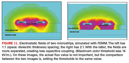
Crosstalk between traces on the same layer. Among several parameters, the trace separation versus dielectric thickness ratio (and not the width versus separation ratio) has a significant effect on crosstalk noise (Figure 11). If the dielectric material (thickness) is changed in the stackup, then the crosstalk levels between the traces change too. If thickness increases but trace-separation remains the same (between traces on the same layer), crosstalk increases. So, if it must be changed on a board post-prototype, only decrease the thicknesses (between signal layer and ground/reference plane); never increase them. Increasing the dielectric thickness will increase the ground return current areas and their overlapping (different signals) area. It also increases the mutual inductance and mutual capacitance. Crosstalk can be traced to mutual inductances and capacitances between traces, so they must remain low. A poor but widespread practice is to allow different fabricators to change the stackup based on their material stock. Material change usually means dielectric thickness change, which changes the crosstalk levels. Typically, those involved are too ill-informed to know they are changing the crosstalk levels too. To avoid problems, a design or signal integrity engineer must be involved in approving new stackups for existing boards, and they have to understand the effects. Otherwise, poor yields or field failures will occur at random.
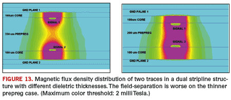
Crosstalk between traces on different layers (dual striplines). Since the two signal layers reside in each other’s magnetic and electrostatic fields (between the same two reference planes), there is a lot of parasitic inductance and capacitance between the traces. A usual technique is to perpendicularly (90°) route the signals on the two layers, avoiding long coupled segments between them. The crosstalk levels (mutual L, C) are higher for longer parallel trace segments. For complex digital boards, it usually is impossible to maintain 90° routing. Do not use dual striplines. (Use more ground planes.) Try to minimize the overlapping areas of the magnetic flux and electrostatic fields (Figure 13) on the two layers to minimize crosstalk. This can be accomplished by putting the signal layers closer to the two different reference planes, and farther from each other. Poor industry practice (changing stackups without approval by hardware or signal integrity engineers) has the same effect on this type of crosstalk as was described in the previous section: changing crosstalk levels without control or attention (indeterminate behavior).
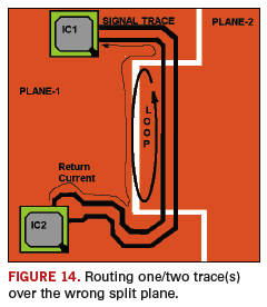
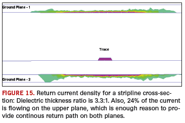
Crosstalk caused by return current discontinuities. When the return currents of multiple traces are forced away from their natural path to a plane-split edge, they induce noise currents into each other’s signals. Since the return current in these cases is not flowing underneath the traces but with a few millimeters offset, they create a current loop. One branch of the loop is the signal (signal current) and the other is the return current (Figure 14). For plane discontinuities, these loops of different signals overlap, and they effectively create a single-turn transformer between the signals, which creates strong crosstalk. The obvious response is to route all signals only above continous planes. Both planes must be continous for striplines, since the return currents flow in both planes (Figure 15).
For stripline structures, provide the current return path in both planes, not only in the closer one, since the return current has its natural path in both planes. For dual striplines, both signal layers have return currents in both planes.
Layer change without stitching vias (or stitching/decoupling capacitors) also belongs to this problem group, since after pulling the signal through the stackup, we also have to provide the return current path through the stackup to the appropriate planes (between the reference planes of the start and the destination signal layers). Impedance discontinuities. The trace impedance will be the same as the calculated value if there is a path provided in (both) the reference plane(s) where the return current can flow. If we cut its way (plane split), or the signal’s driver or receiver chip’s ground pin has no short (AC) connection to the reference plane(s), or there are voids on the plane (antipads), then the return current is forced away from its natuaral path (right underneath the signal trace with a specific current distribution shape), and the calculated impedance is no longer valid. It is a simplification to say the impedance is defined by the PCB cross-section geometry. In reality, it is defined by the shape of the distributed currents in both the trace and reference planes, and by the shape of the magnetic and electrostatic fields. These field shapes are guided by the geometry.
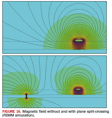
For example, a 100 µm wide microstrip trace over a 100 µm dielectric has an impedance on 1 GHz of 69.5Ω (based on FEMM RLGC simulation), but when the trace has to cross a plane split and go above the wrong plane in parallel to the split edge at a distance of 9 mm for awhile, then the impedance will be 158.9Ω, a huge difference (Figure 16). The reason is the modified current return path inside the reference planes, which increases ground path inductance. Another reason is that the trace capacitance (electrostatic field) now has to go through the plane split too, so the C parameter is decreased. If there is a big void on a reference plane, it creates the same problem: The return current cannot jump to the next plane for that part of the signal path, but only flows on continuous copper. In some cases (not between analog and noisy-digital grounds), this return current path can be provided by using stitching capacitors over the split.
The two main reasons why discontinuities are bad are 1) if 50Ω are needed and 150Ω are obtained, then obviously the impedance requirements are not met, and 2) discontinuities also significantly increase crosstalk and EMI.
3-D discontinuities. Via transitions, connectors and IC package pins create 3-D discontinuities that only can be modeled by 3-D electromagnetic simulators (e.g., Agilent Momentum, Ansoft HFSS, CST Microwave Studio, Cray-LC). These 3-D discontinuities create impedance deviation from the simply calculated values, and introduce parasitic inductances and capacitances into the signal path. The previously described discontinuities also are 3-D, but are so flat, they can be handled as 2-D discontinuities.
Conclusions Not only must cross-section parameters be taken into account, but also other layers in the stackup, reference plane discontinuities, the used signals, the pattern on the copper layers, and so on. Because higher signaling speeds require better signal integrity, impedance control for today’s multi-GHz or multi-Gb boards has to involve more knowledge (PCB manufacturing technologies, high-frequency measurements, signal integrity, electromagnetism, material science) and more sophisticated tools than was necessary even a few years ago. One part of maintaining good signal integrity is to control impedances within a tight range.
For a quick way to perform everyday calculations for design, use a frequency-independent method for simplicity, with a few parameters considered on an average or usual constant signaling frequency. For computer motherboard designs, 2 GHz seems to give the best accuracy. The fully frequency-dependent method is not completely developed, especially not from the design point of view. It may be used for analysis for verifying the impedances. PCD&F
References 10. Simberian Inc., “Micro-strip Line Characteristic Impedance and TDR,” application note #2009_04, April 2009. 11. Mayo Clinic Special Purpose Processor Development Group, TNT MMTL freeware field solver program, http://mmtl.sourceforge.net/. 12. Applied Simulation Technology (Apsim), AppCAD RLGC, http://apsimtech.com/. 13. The field-simulations in this document were prepared in the Finite Element Method Magnetics (FEMM) freeware/opensource 2-D fieldsolver program (http://femm. foster-miller.net).
Istvan Nagy is hardware design engineer at Concurrent Technologies (cct.co.uk); This email address is being protected from spambots. You need JavaScript enabled to view it..
The right impedance ensures against additional SI or EMI issues.
A well-designed power distribution network (PDN) must have low impedance on the delivery path. The question is, How “low” is enough so that a PDN can deliver sufficient power supply for ICs to work properly? To answer this, we first need to define the impedance so that a PDN can be mathematically represented.
Suppose a PDN to be a linear network with named nodes and branches, and current flowing from VRM through PDN to ICs. The impedance at any location of a PDN can be defined as
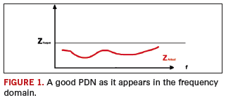
The impedance here is the ratio of actual node voltage change to the total dynamic current drawn by ICs at any frequency point. If the total current is normalized as 1, the node voltage at any location gives the impedance at that node. At a given frequency, when x and y are the coordinates of IC power supply pins, the impedance would be the one seen by an IC component to the PDN, which is what board or system designers are interested in, and needs to be minimized. Figure 1 illustrates a good PDN as it appears in the frequency domain.
It is important to emphasize the PDN impedance is defined in frequency domain. Then, how do we use it in a digital design, which works with transient signals in time domain?
Time domain considerations. Considering the power supply for an IC needs to be steady at a required DC level, and the IC can tolerate certain variation of DC voltage (ripple and sag), the DC voltage level and the tolerance give the variation range of power supply. Since the voltage changes in the time domain consist of frequency components at all frequencies, the goal of a PDN design can be described by the minimum range of voltage changes, and maximum current drawn by ICs. This is what we call the target impedance Zt
Here, the supply voltage and allowed ripples (in percentage) give the power supply budget, and the current is the worst transient current drawn by ICs connecting to PDN. Because voltage ripples and the worst transient current can happen at any frequency, this makes the target impedance independent of frequency. In practice, the target impedance, which is effective at all frequencies, is neither achievable nor necessary due to the limited switching speed of a physical IC.
Because the voltage ripples are caused by the combination of the switching currents of all ICs, which a PDN needs to provide power to, the term “current” in Eq. 2 represents actually the total allowable current to switch at the same time. It does not identify when and where individual switching currents occur. From this point, the target impedance in (2) is rather pessimistic; a design meeting the target impedance of (2) may not be an efficient one.
In high-speed digital designs, chips switch their states in sequence. Therefore, all switching current has its profile in time domain. When switching current with a certain profile happens, it means a time variation current source is applied to a PDN at one or several ports (IC power pins). This current induces voltage drops across PDN, which reveals the actual voltage a chip will get during its state changes.
The last question on IC current would be where a PDN designer can obtain switching current profiles. As discussed, the switching current represents the dynamic power consumption on chip, which consists of core and I/Os. Considering the simulation tools for board or package have no access to the IC database, and the chip structure is generally beyond the scale of board/package tools’ solving capacity, the best approach for getting accurate switching current profiles is to contact IC manufacturers that own power analysis tools and measurement equipment for chips. Fortunately, IC manufacturers are willing to provide such information to system designers.
One last caveat: This discussion about PDN impedance assumes a power delivery path ends at the BGA of a component mounting on a printed circuit board, and IC current is drawn directly at BGAs. In reality, the actual component on board includes chip and package, which introduce additional inductance and capacitance to be resonant with the rest of the PDN impedance. Package parasitics and on-die capacitance can be included in PDN if both models are available. However, the new PDN impedance becomes “component-dependent.” If a component is replaced by another, the impedance of the entire PDN needs to be reanalyzed. A better solution is to equip PI tools with user-preferred options about package and chip effects.
Although power integrity is relatively a new term in high-speed digital design and analysis, its concept has been used in designs for many years. The goal of power integrity is to have PDN provide sufficient power supply to ICs efficiently, without introducing additional SI or EMI problems. The important means to designing a good PDN is to make PDN impedance below predefined target impedance. PCD&F
Dr. Zhen Mu is product market manager at Mentor Graphics (mentor.com).