Recent horror stories remind us that designers really need to know it all.
A recent blog on the Circuits Assembly websitegot me going on one of my pet topics. This will come as no surprise to those of you who know me, but once I overcome inertia and a latent proclivity for procrastination, I usually have to take a nap, thanks to all the effort of overcoming said inertia and procrastination.
But not this time.
This time the subject close to my heart is design for manufacture. The blog, written by regular contributor Duane Benson of Screaming Circuits, is titled “Another Land Pattern Mixup." It is just so difficult to understand how, after all this time, we still cannot get right certain fundamental things between design and manufacturing.
Now I won’t pretend to know the particulars here. There may have been a mistake when the part was created; the part number may have changed somewhere along the line, or someone at the CAM station may have screwed up. I don’t know. But I do know that here is a board that has a land pattern that will not accommodate the component supposed to go in the circuit.
Duane also shows an example of what looks like a jumper strip that is probably a metric part, but at first glance, it appears the designer used imperial dimensions. It probably would work if there were only a few pins, but over the length of 11 pins, the conversion round off or tolerance means the part won’t fit into the board. At first blush, we naturally would say the designer screwed up. But what if somewhere along the line, purchasing or some other entity substituted a part that “looked the same” to save a penny or two? In many companies, a librarian is responsible for creating the footprints. Sometimes this person is not a designer or does not really understand all the implications of what they are doing. Whatever the cause, there is a preventable problem here.
I’m not going to put all the blame on the designer because the truth is, in many cases, neither side of this issue really understands the fundamentals of the other. Many people in manufacturing really do not understand who the designer is, much less what they really do. The only thing they know about the designer is what they read in the media or see in the Gerber files. And before we go further, I’ll add that, yes, some folks in the media write about design and manufacture and don’t know who or what the designer (or the fabricator, for that matter) is. They may fool some folks, but designers usually can tell the difference between those who have had to find a way to connect those last few traces and those who have not.
When it really gets down to where solder meets laminate, the buck stops at the designer. No matter what the problem is, more than likely whoever designed theboard is going to take the rap. In most cases, that is as it should be. Fabricators and assemblers may not need to know how to design a board, but designers need to know how every aspect of the PCB manufacturing process affects their decisions. One of my drafting gurus told me that, after I finished a drawing, I should stand back, look at the drawing, and ask myself if I could build the part from the information on the paper (yes, paper; it was the 1970s). The catch here is that if you don’t know what happens in the shop, you can’t answer those questions.
Over the past 20 years, PCD&F and Circuits Assembly have published countless articles about DfM. We’ve produced scores of classes at the PCB Design Conferences, and I’d like to think many designers know a lot more about manufacturing than they did before they read those articles or attended those classes. So it boggles my mind that we still see the kinds of problems Duane points out.
I know there are pressures to get the design out now! A host of other issues play into this as well. But what good is a design done quickly, if it has this type of problem? What’s the cost of doing another run of prototypes, both in dollars (or euros or yuan) and time? Every manager and bean-counter should be required to read Duane’s blogs and other horror stories, so they have a better understanding of repercussions of decisions made in the design process.
Having made those claims about our attempts to eliminate DfM problems, I’ll still take some of the blame. Our mission includes educating and bringing the sides together. Evidently we haven’t done a good enough job of that. In the coming months, we’re going to recommit to this mission. But it has to be something in addition to articles and sessions at our shows. Those are important parts of the puzzle, but we need more. Next month, I’ll let you in on what I have in mind.
Until then, stay in touch and, as humorist and author Tom Bodett says, we’ll leave a light on for you. PCD&F
Pete Waddell is design technical editor of PCD&F (pcdandf.com); This email address is being protected from spambots. You need JavaScript enabled to view it..
Merger mania strikes again. Will it play out differently this time?
Just when you thought it was safe, along comes déjà vu all over again!
In so many ways, our industry looks much different as we embark on the second decade of the “new millennium” than it did in the last decade of the past one. Fewer companies are competing, and there is a very different global geographic distribution. Quality and on-time delivery – every company’s means for dramatic improvement a decade ago – are no longer differentiators, as everyone has dramatically improved and performs equally. Technology itself has marched along so quickly that what was “cutting-edge” a decade ago would be considered “commodity” today. But in one way the 1990s are alive and well: Merger mania has once again struck industry boardrooms.
For those who may not remember (or who wisely forgot!), in the mid 1990s a buyout group began a rollup of smaller (albeit what in today’s world would be considered large) companies into what is now Viasystems. On the heels of this business model, and with the encouragement of some of the then-brightest Wall Street analysts who covered our industry, others followed suit. Remember Hadco and Praegitzer? They were caught up in the mania, as was DDI, Altron, Continental Circuits (the Phoenix version), Coretec and a host of much smaller and all-but-forgotten companies.
Like many, I have fond memories of the halcyon ’90s. And I’m not necessarily against mergers; in fact, if someone came along with a boatload of money, I too might sell in the proverbial New York minute. But looking at the carnage, and considering the cost vs. value of those transactions, I have to ask, “What are you guys thinking?!” If the mantra of the ’90s was quality and on-time delivery, the mantra of the new millennium has been “value,” and it takes some stretch to understand how most mergers create value. Early in my corporate career, I was responsible for “business planning,” which included mergers and acquisitions. Being with a Fortune 100 corporation, we sold a lot of businesses that no longer fit with our ever-changing corporate “vision” of businesses – usually selling poorly managed or neglected facilities.
We never seemed to do well buying other companies either. Too often after closing a deal, we would soon find that the culture, capability and claimed strengths of what we had just bought weren’t quite as advertised. More than a few acquired facilities quickly made their way to the list of poorly managed or neglected facilities that were sold! The exceptions were the few cases where the acquired facility filled a specific niche, or where we could shut down the facility and assimilate the business into an existing, better-managed facility. My take from a few years buying and selling was that, once all the dust settled from the deal, rarely was any value gained.
Looking back at the volumes of merger activity, I believe the same was true: little or no real value resulted from all the deals. Surely most companies actively in the hunt for deals are no longer in business. More telling, the capacity footprint is a shadow of its former self, both for the companies involved in those mergers and the industry as a whole.
What is different this time? Instead of the heady, egocentric hype of last decade, this round has been lower key, keeping with the economic mood of the times. In some ways today’s transactions appear more like a hybrid of Jack the Ripper meets Pac Man. But the results appear headed to the same conclusion, which is to say that little, if any real value will result from the (sizable) investments made.
This brings me back to the déjà vu aspect of today’s merger environment. Several of the megadeals have involved the same companies who lost so much the last time they forayed into the M&A world. You would think they would have learned that as attractive as an acquisition may appear, the end-results don’t always warrant the time, talent and treasure initially invested and subsequently required. More to the point, in an industry that has a voracious appetite for investment in technology and the capital equipment to produce it, maybe money can and should be better spent building the competence of a company’s technology franchise in order to build value.
Customers are searching for technology solutions – answers – for the next generation of product. Building value requires being able to invest in and develop technology. Equally, as the equipment used by many in our industry is getting long in the tooth, investing in more, older equipment and infrastructure via an acquisition heightens the risk.
Some may say that merging large companies will increase value by consolidating excess capacity or reducing the unsustainable “desperation” pricing that sometimes results when weaker companies make last-ditch efforts to fill plants. However, if those involved are that weak, they eventually will founder, and the same result achieved with no investment required.
I do hope this time around, these mergers have a happier ending. In each case, hopefully the acquiring company really needs additional capacity and capability, and the corporate culture fits with their needs and actually increases value for all.
But we should keep in mind the companies that survived previous downturns were, and are, ones that regardless of size or location have remained focused on building value by satisfying customer needs. And customers need technology development and solutions for tomorrow’s products. The greatest single value-adding strategy any company can follow is to stick to its knitting and invest in developing the technology and capability to service customers and their markets. PCD&F
Peter Bigelow is president and CEO of IMI (imipcb.com); This email address is being protected from spambots. You need JavaScript enabled to view it.. His column appears monthly.
At the risk of beating the tin drum (and wasn’t that movie painful enough to sit through?) once too often, I will mine (get it?) the Conflict Metals subject one last time.
To recap, Conflict Metals refer to ores extracted from the battle-raged Democratic Republic of Congo, where millions of citizens have died, casualties of a fierce civil war underwritten in part by revenues from contested mining activities.
Following my last two columns, I have heard from various sources who hoped to refine my thinking. One noted that the Congo supplies less than 5% of the world’s tin, suggesting the electronics industry, which as these things go is hardly a major consumer of the metal (some estimates put electronics’ share at 2% of the global consumption), could survive just fine without the DRC as a source. (By the way, tin owns no patent on the issue. The DRC also sits on large deposits of tantalum.)
Second, while the audits proposed by the International Tin Research Institute and other similar-thinking groups (see last month’s Caveat Lector) are a step in the right direction, in some cases they are redundant with existing corporate practice. And reclaimed materials are exempt from the discussion, because, among other reasons, the alternative would be to landfill the disputed metal. As Cookson Electronics president Steve Corbett, one of the few willing to speak on the record, told me, “Customers are not looking for verification on reclaimed materials. And we say, ‘You really don’t want to throw a wet blanket on reclaim, because you want to keep it out of landfills.’ ”
In that sense, even the most intense certification programs are inherently incomplete. While some companies would be able to guarantee there are, in the words of one colorful source, “no Congolese atoms” in their products, there simply is no way for industry as a whole to ensure its products contain no amount of Conflict Metals.
In the US and elsewhere, pending legislation – which one source called “ludicrous” – emits the radioactive notion that through industry pressure, governments can solve the civil war. “According to the politicians, there are legitimate mines,” said one solder supplier. “It’s like the cotton picking of the Civil War: the South cotton is bad; the North is OK. We’re picking sides in a civil war in Africa.”
Nevertheless, it would be a mischaracterization to suggest solder vendors are simply throwing up their hands in despair. Solder suppliers are actively trying to determine if their smelters use ores from the DRC and, if so, remove scofflaws from their vendor lists.
It’s true the industry cannot determine which tin atoms came from where. Still, pressure is heavy from OEMs like Nokia, H-P and Intel that wear their respective corporate social responsibility (CSR) statements like a badge. That could explain why solder suppliers aren’t balking at ITRI’s proposal to add $50 a tonne to underwrite compliance audits, as they seem intent on passing those costs along to customers that demand the audits.
But I came away certain that the industry should push back on this issue. This approach should be twofold: First, it should use governmental channels. Though IPC might be too small to be effective, the National Association of Manufacturers (NAM) or the National Association of Surface Finishers (NASF) might be a good place to start. (If you can put a good spin on hexavalent chromium, what can’t you do?) Second, it needs to attack the exchanges.
According to my sources, the London Metal Exchange will not certify that the metals in its warehouses are free of Conflict Metals. Solder vendors should collaborate to remedy this, for if the LME doesn’t comply, the effort toward compliance will be uncertain, at best.
Finally, I should clarify that not every solder supplier buys raw materials from the exchanges. Some buy direct from smelters. My apologies for suggesting otherwise. Jumping, but not for joy. I’m old enough to remember the old Toyota commercials where everybody would jump into the air at the end, and the voiceover would say, “Oh, what a feeling!” Well, Toyota has made car owners jumpy again, but not with pleasure. As I write, the nation’s media and blogosphere is afire with speculation over what is to blame for the automaker’s sudden acceleration problems. Some, including Dr. Michael Pecht of University of Maryland’s Center for Advanced Life Cycle Engineering (CALCE), are pointing to a breakdown in the electronics throttle system. Which begs the question, are the much-publicized recalls tied to a lead-free problem?
Bob Landman, a reliability expert and a Life Senior Member of IEEE, has been vocal that the connection between lead-free solder and tin whiskers is both real and potentially deadly. He asserts “the increased use of electronics in automobiles when mixed with RoHS can make for a deadly cocktail. We don’t know what the causative agent [in regard to the Toyota recalls] was, but I have heard recently of new autos showing up at dealers that will not start. That cause has been linked to tin whiskers.”
We do not yet have enough information to determine whether tin whiskers or even lead-free solders are at issue here. One would hope Toyota comes clean, if indeed the true cause can be determined, so that the industry at large can learn from their mistakes.
P.S. Landman moderated a chat on tin whiskers during Virtual PCB this month. See the transcript on-demand at www.virtual-pcb.com.
What happens to CAD data once they are released to manufacturing?
How often does the fabrication drawing have a note that states something similar to this?
“DATA MAY NOT BE MODIFIED WITHOUT WRITTEN APPROVAL.”
Is it your intention that the board fabricator should make production tools from your data “AS IS” and run with it? If not, do you have a clear idea what modifications are acceptable?
Let’s imagine our responsibilities if we were working in the CAM department of a board manufacturer. Our customers are using different software tools for circuit board layout, using different rules and parameters, and creating output data in different formats. We can’t expect any two customers would do the same thing the same way. Our job would be to:
Accept data from many sources.
Analyze the data and customer requirements.
Prove they are acceptable for our process.
Modify the data, as needed.
Output the data to consistent formats.
Insert data as a smoothly running stream into manufacturing.
I recently had the opportunity to learn more about what happens to our data once we let go of it. I followed a typical job from our facility through manufacturing, and this is what happened.
Step 1, Data discovery. After the data passed through the Sales and Quoting department to Front-End Engineering, Frontline Genesis 2000 software was used to import it. (Other systems perform similar functions, and this process is not tied to any particular CAD or CAM software.)
Because designers have a variety of naming conventions for files, most CAM systems have a feature that automatically examines the file internally to interpret the data type and format settings. The software’s “best guess” is displayed on the screen. Once they are identified correctly, the artwork layers and drilling data are often renamed or labeled for consistency or to aid subsequent processes.
If there are any missing files, files that won’t load or obvious data errors, the job is put “ON HOLD” and the customer is notified.
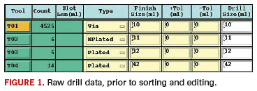
Step 2, Data manipulation. The first step is to ensure all artwork layers are aligned. Then drill data are compared to the hole chart on the fabrication drawing (Figure 1), and, if everything matches, the data are sorted into plated and unplated holes. (They are used at different times in the board fabrication process.)
Unplated drills are moved to a separate layer, and any copper target pads removed from their centers. Also, in our case the design was an array of multiple images, but the drill files were output as “one up,” so the drills had to be copied in a “step-and-repeat” pattern to match the artwork.
Any copper or silkscreen features that cross the board outline will be clipped to within 0.010˝ of the edge. Text or other drawn features outside the board edge will be removed.
If a netlist can be extracted from the CAD data, or if one is provided (preferably in IPC-D-356 format), it is compared to a netlist generated directly from the Gerber data, to look for discrepancies. If any mismatches are found, the job is placed “ON HOLD” and the customer is notified.
The following edits are made to improve the speed and accuracy of the design rule checks (DRC) performed in the next step:
Arcs created with a series of short segments are converted to a single smooth drawn arc.
Pads created with draws are converted to flashes.
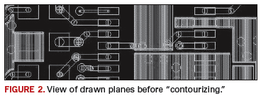
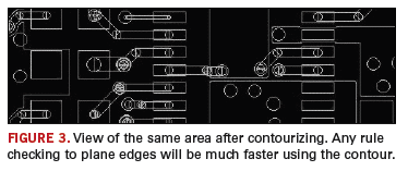
Planes created with draws are converted to a single polygon contour (Figures 2 and 3).
Legend detection identifies text on conductive layers, so the checking process won’t flag them as “hanging traces.”
SMD attributes detection identifies “pads without drills” to be understood as endpoints for netlist-checking later.
At this point, the netlist is re-verified to ensure any unintentional editing hasn’t altered the design integrity.
Step 3, Data verification. During this phase, several different rules are used to check the design, to ensure variations in fabrication processes will still produce a reliable circuit board. These rules are typically set by default in the CAM system, but are often customized to meet the unique requirements of the customer. Here’s what happened to my design:
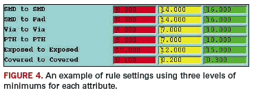
The minimum clearances and trace widths were identified. In our example, widths and clearances were collected and sorted into three categories: green, yellow and red. The green were OK, of course, but the yellow instances were approaching limits, and the red items highlighted the need for cost/yield considerations and maybe even the need to put the job on hold and consult with the customer (Figure 4).
The profile was checked. Measured were the copper feature distance to board edge, contours, cutouts and unplated holes (0.010˝ min.).
Drill diameters were compared to copper pad sizes to ensure sufficient annular ring for minimum acceptability.
Stubs and hangers were located and removed (or reported to the customer).
Step 4, Data preparation. Final modifications are then made to the data before they are sent to fabrication:
Solder resist layers are examined to see if apertures have been expanded or supplied as 1:1 match with copper. Modifications here may shrink or expand mask as necessary, and dam slivers may be removed, especially around fine-pitch SMT land patterns.
Silkscreen legend/nomenclature is clipped from exposed copper (solderable) surfaces, using the soldermask edges as a boundary/cutting edge.
Nonfunctional pads may be removed, depending on the default practices of the supplier or customer requirements.
Trace widths and/or dielectric spacing will be tuned to meet impedance requirements.
Compensation – copper feature dimensions may be increased to compensate for etching processes.
Pad teardropping may be added to reduce drill breakout in “conductor to land” junction area.
Company logo/UL marking and date code added to design.
Step 5, Data output. The data manipulation described in Step 4 was applied to the design as-received, while the following steps describe further manipulation to convert the design into production-ready tools. It would be difficult to list every possible variation, but every job will have a subset of these steps and have the same desired result (a working board that meets the customer’s requirements for the highest yield at the cheapest cost):
Individual or “palletized” designs (multiple boards placed in a single frame for ease of assembly) are arranged on the fabrication panel size (step and repeat).
Layers may be “stretched” to compensate for fabrication process tolerances downstream.
Tooling features, thieving and tracking/identification added.
Milling data are created to excise the final product from the fabrication panel.
Files for final electrical test are generated.
Layers in the “bottom half” of the stackup are mirrored.
The final task of Front-End Engineering is to output the final data into formats required by the specific fabrication equipment, and (if step-and-repeat was performed during CAM instead of CAD) send paste screen and palletization data to the customer.
Q&A
I asked several questions and discussed the answers with the FrontLine Users Group and several online discussion forums. This is a summary:
CAD: As designers, we are taught to define the data origin on a tooling hole if possible, but I never saw you use it for anything.
CAM: Maybe the origin is useful to someone down the line, but not to us. What’s more important is for all layers to have the same origin so they stack up correctly, including the drills.
CAD: I noticed you didn’t use the milling data we sent for routing the profile of the board. Why was that?
CAM: We don’t get that type of data very often. When we do, they usually are not optimized for manufacturing, and we have to modify them to minimize the tool path. It’s a simple matter to create, so don’t waste your time trying to provide it for us.
CAD: I noticed you changed the width of the features drawn on the silkscreen layers. Why was that?
CAM: From our experience, the customer doesn’t care about the width specifically; they just want it to be legible. Depending on the letter height, we adjust the width to work well in our process and give consistent results.
CAD: When you receive a note stating, “Data may not be modified without written approval,” do you perform the CAM job any differently?
CAM: Usually not. There are things we have to do to give you a good product, and the intention of the note does not pertain to those. Some customers are more than happy to have us fix things we find as part of the service we provide, but others would rather fix it themselves and send new data. Either way is fine with us, and learning each customer’s expectations is part of building a good relationship. Of course, we rely on written communications in all situations.
CAD: If you had one wish for improving the CAD-to-CAM process, what would it be?
CAM: (This is the only question that got multiple answers, which varied from “intelligent format” to “have every CAD operator spend a month in CAM, and every CAM operator spend a month on the shop floor” to “free ice-cream on Fridays.”)
Recommendations
Here are ideas for making this process more efficient and less susceptible to error. If possible, submit data in an intelligent format such as ODB++, but make sure the CAD system has implemented a reliable export capability. If you’re not sure, send a test file to prove your manufacturing partners can import it without difficulty.
(You may want to create Gerber data in parallel as a backup for suppliers who can’t import an intelligent format.)
If Gerber data must be sent:
Ensure the artwork layers and drilling files are created using the same format. (If you don’t know what to use, you probably can’t go wrong specifying ABSOLUTE, NO ZERO SUPRESSION and either 2:6 for coordinates in inches or 3:3 if the units are in metric.)
Create a separate layer for the board outline, or plot it only for the soldermask layers. You don’t want etched copper board outlines on every layer, or on the finished silkscreen.
Unless you are an expert, generate soldermask openings 1:1 with the pad sizes (except for fiducials). Unless the designer is known to have paid careful attention to expanding the soldermask apertures appropriately, the manufacturer would rather do it using a known starting place. Starting with mask that matches the pads makes the modification process much easier for the manufacturer.
If you are OK with removing nonfunctional pads, leave them in the design so they can be used for drill/annular ring checking, and the CAM operator can remove them later.
A unique aperture size used to draw planes, sized differently than any of the thermal spoke widths, can be very helpful to CAM.
Differentiate which holes are plated and which are unplated.
If leaving it to CAM to create an assembly array or pallet with breakaway tabs, make sure to leave spaces free of traces and components for the tabs.
ReadMe files are encouraged! Make sure to list any known netlist discrepancies.
Never try to perform your own etch compensation!
Finally, preview the final output before you send it out. You can find several free tools by searching the Web for “Gerber viewer.”
Jack Olson, CID+, is a circuit board designer at Caterpillar Inc. (caterpillar.com); This email address is being protected from spambots. You need JavaScript enabled to view it.. Mike Tucker is a technical service engineer at P.D. Circuits (pdcircuits.com).
Written by Hiroshi Hoshiyama, Shinjiroh Hayashi, Makoto Sakai and Rikiya Shimizu
Category: 2010 Issues
A novel process is said to improve product interconnection and mechanical reliability.
Today, the most common flexible printed circuit substrates are 12.5 - 25 µm thick, with the trend toward even thinner materials. Two primary types of copper foil are used for flex: electrolytic copper foil and rolled copper foil. Electrolytic copper foils typically come in thicknesses of 18 or 12 µm, while most rolled copper foils are 18 µm thick. As with polyimide substrates, both types of copper foils are moving to thinner dimensions. Generally, rolled copper foils demonstrate flexural properties superior to those of electrolytic copper foil. Applications that require very high degrees of flexibility and reliability, such as HDD read-write heads, are dominated by rolled copper foils. However, in recent years, the flexural properties of electrolytic copper foil have been greatly improved and are gaining share in optical pickup applications.
Each of the three FPC categories – single-sided, double-sided, multilayer – requires somewhat different manufacturing processes. In addition, manufacturing processes for multilayer FPCs vary significantly, depending on the specifics of the desired circuit structure and performance characteristics.
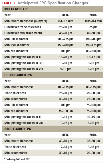
Table 1 demonstrates the evolution of FPC specifications. Design rules are changing to support miniaturization and multi-functionality. Trace widths and board thicknesses are becoming smaller. Minimum plating thicknesses are falling, leading to higher demands on the performance of plated copper deposits.
During double-sided/multilayer FPC manufacturing, metallization is employed to provide robust electric connections between layers. These processes represent critical steps within the overall production sequence. Typically, a combination of electroless copper plating and electrolytic copper plating is used to form plated through-holes and vias. Direct plate processes also are now widely used for initial metallization prior to electrolytic copper plating, especially for double-sided FPC.
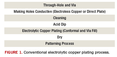
Electrolytic copper plating has a significant impact on FPC manufacture, as it affects wiring design, board dimensional tolerances and thermal/mechanical reliability. Figure 1 illustrates a conventional process flow for electrolytic copper plating. Electrolytic copper plating is carried out after the process steps of through-hole/via-hole formation, initial metallization process and pre-cleaning. Plated panels are dried prior to the patterning process. Since FPCs are thin and flexible, these features must be considered in their design and handling.
Electroplated copper deposits must have the following characteristics:
Dimensional stability after plating (ensures stable wiring dimensions).
Thermal/mechanical reliability (delivers appropriate performance for end-use environment and device assembly).
Compatible with full range of making holes conductive chemistries.
Uniform plating distribution on board surface (allows consistent circuit feature formation).
Plating surface smoothness (eliminates surface defects that might reduce manufacturing yield or degrade flexural performance).
Trends toward finer feature dimensions and higher interconnection densities require improved functionality from FPC electrolytic copper plating processes.
The attributes and benefits of a new electrolytic copper plating process are illustrated by comparison with the performance of conventional processes.
Dimensional stability. In response to finer feature and higher interconnection density trends, registration tolerance has to be improved. Improved substrate dimensional stability during manufacturing is required to meet these targets for registration tolerance. The main factors affecting dimensional stability during FPC manufacturing are base material performance, plating deposit properties and manufacturing process conditions. Internal stress within electrolytic copper plating deposits plays an important part in determining the overall dimensional stability. The effect of plating stress manifests itself as either bowing of boards after etching or patterning, or as shifts in pattern feature locations. The board dimensions shrink when the deposit has tensile deposit stress and expands under compressive stress. FPCs are particularly influenced by internal stress because the boards are so thin and flexible.
Typically, the internal stress of acid copper deposits is tensile. The amount of internal stress changes gradually, due to structural changes associated with self-annealing of the deposit. A copper plating process having low internal stress is therefore preferred for FPC applications.
A spiral contractometer is most commonly used to measure stress in plated coatings. The deposit is formed on the exterior surface of a spiral shaped metal substrate, which is tightly secured at the lower end but free to move at the upper end. The interior surface is coated with an organic material to prevent deposition. Stresses within the deposit lead to either an opening or a tightening of the spriral, measured as an angular deflection of an indicator connected to the upper end. The deflection, combined with information on deposit thickness, then can be converted into a value for stress.
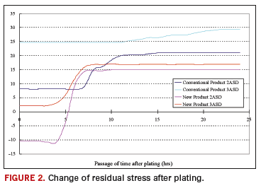
Figure 2 shows the residual stress for a conventional plating system and a newly developed bath, as a function of time after plating and plating current density. In a conventional process, deposit internal stress stabilizes between 20 - 30 MPa after 10 hr. While this level of residual stress is unlikely to have significant impacts on present FPC designs, it presents an issue for future design specifications. The new process shows an internal stress that reaches a value of approximately 15 MPa after 7 hr., and then remains stable. The residual stress is significantly lower than conventional processes.
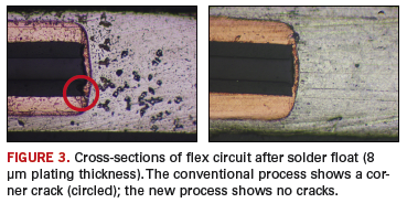
Thermal/mechanical reliability. Pb-free processing means higher assembly temperatures, placing greater demands on thermal reliability. The physical properties of electrolytic copper plating deposits must be enhanced to respond to these changes in assembly conditions and the trend toward finer feature dimensions. Figure 3 shows cross-sections of through-holes in FPCs after solder float testing and describes the substrate construction and test procedure. In general, when the plated deposits are thin (as is often the case in FPC applications), interconnection failures such as cracks tend to occur as a result of thermal shock. In tests, the new product shows excellent performance, even when used at low plating thicknesses. This provides an improved process window during assembly operations.
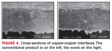
Compatibility with alternative metallization processes. Direct plating processes are widely used for the initial metallization of general-purpose, double-sided FPC. Compared to electroless copper plating, the resistance of the initial direct plate film is high, which poses a risk of deposition failure in the subsequent electrolytic copper plating process. In such cases, powdery copper deposits may be formed during the early stages of plating, resulting in adhesion defects and poor appearance. The new process has been found to show excellent compatibility with both a wide range of electroless copper and direct plate processes, providing excellent copper-to-copper interface quality (Figure 4).
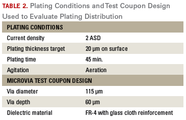
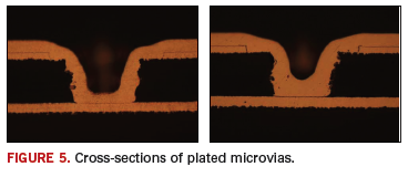
Plating distribution. Thinner copper foils and plated copper deposits and microvias are essential for increasing circuit density. High-density multilayer FPCs employ microvias for innerlayer connections. Consistent and uniform plating distribution is required to ensure optimum connection reliability, particularly for smaller diameter microvias (Table 2). Figure 5 compares coverage capabilities of electrolytic copper plating on microvias. The new process shows improved capability, even for small diameter vias, due to its plating coverage and distribution.
Surface smoothness. In contrast to rigid boards, FPCs require very high degrees of deposit flexibility. Bend test requirements for the FPC section that acts as an interconnection between boards vary widely with application. In the case of the interconnection within the hinge of a cell phone, more than 100,000 flexures are required (measured using a 180° open/close test).2
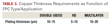
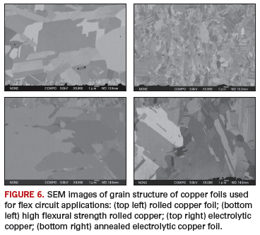
The area undergoing the bending operation must have a thin copper deposit in order to meet these needs. Table 3 shows examples of typical electrolytic copper plating thicknesses as a function of FPC type. FPCs used for moving parts generally use rolled copper foils, due to their superior bending performance. However, when electrolytic copper plating is applied over rolled copper foil, some degree of surface unevenness can sometimes be observed on the plated deposit. This is believed caused by an interaction between the plating process and the crystal structure of the foil substrate (Figure 6).
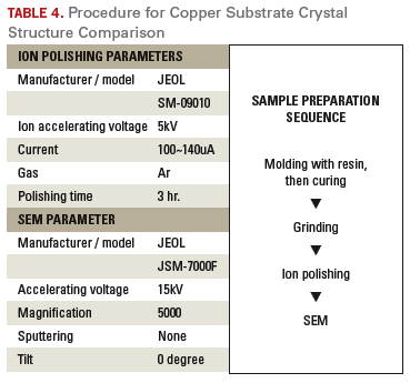
Ion polishing was used to prepare samples, which illustrate the differences in crystal structures between four different copper substrate materials (Table 4).
Unannealed electrolytic foils have relatively smaller grain sizes, while the grain sizes of rolled or annealed electroplated foils are larger (Figure 6).
Surface unevenness may lead to defects in subsequent imaging processes and can therefore become a major obstacle to high yield manufacture of finer line high-density FPC. To reduce the unevenness, higher plating thicknesses or mechanical polishing have been considered. However, thicker films have been observed to degrade flexural performance, and mechanical polishing is very difficult to perform, due to flex’s thin and soft properties. Electrolytic copper plating processes are required to produce deposits with excellent surface smoothness on all copper foils used for FPC to permit finer patterning and higher bending performance at reduced deposition thicknesses and without mechanical polishing.
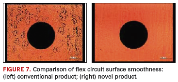
When plating on rolled copper foils, conventional products often show some fine surface unevenness and a semi-bright appearance. In contrast, no surface unevenness is found with the novel product and good brightness is observed. The new process permits reduced plating thicknesses with excellent plated surface smoothness, which provides both fine patterning capability and improved flexural performance.
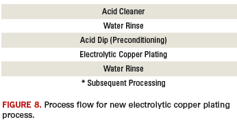
Figure 7 shows a comparison of deposit brightness between a conventional process and the new process. The latter does not require special process control, and conventional plating equipment may be used. Figure 8 shows the process flow of the new electrolytic copper plating.
Ed.: Portions of this article were previously published.
References
1. Japan Jisso Technology Roadmap 2007, pp. 55-57, 63-65, 69-70. 2. M. Watanabe, H. Sakurai, and T. Kanagawa, ”The Future Trend and Characteristics of FPC,” Fujikura Gihou, vol. 109, pg. 33-34, 2005.
Hiroshi Hoshiyama is interconnect technology R&D director Japan; Shinjiroh Hayashi is interconnect technology R&D project leader; Makoto Sakai is interconnect technology R&D scientist, and Rikiya Shimizu is interconnect technology Japan/Korea marketing manager at Rohm and Haas Electronic Materials KK, a Dow Group Co. (rohmhaas.com).
That wonderful RF spectrum may offer functionality and job security.
Recently I was talking to my friend Charley Capers of Trilogy Circuits in Dallas. Charley and I talk regularly on what’s going on in the PCB world and, of course, to stay current on our beloved Dallas Cowboys. (I am writing this the week after they won their first playoff game. If things don’t go well, you may hear some cursing by the time this comes out.) Charley mentioned that Trilogy has carved out a nice niche in RF design. This struck a chord with me because I remember doing some RF and microwave designs back in the 1980s. Then, we talked in terms of 1 GHz. Charley, however, was talking about frequencies in the multiple gigahertz range. This piqued my interest, so I started calling around.
It turns out that while RF may not be considered mainstream right now, it does account for a lot of designs. RFID is one technology that comes to mind, but with the exception of some silicon-based RFIDs, it is considered by most to be a low-tech design. But if you consider all the commercial products that use wireless communications, you’re still talking about a lot of circuit boards. Looking at the top of my desk, there’s a cellphone, the wireless connection to my server, a wireless printer, a Bluetooth headset for the cellphone, and a wireless keyboard and mouse. If I were to inventory my house and office, I’m sure I would find quite a few more wireless applications.
Of course, those applications are all in the 2.5 GHz range or less. Charley was talking about designs in the 10 GHz range and higher. According to my old frequency spectrum chart, “superhigh” or microwave frequencies start around 3 GHz, and “extremely high” frequencies (EHF) start around 30 GHz and go up to around 300. The designs Charley refers to are military applications such as radar, missiles and guidance control systems. But others such as airport x-ray scanners are becoming part of our everyday world and will incorporate frequencies in the RF and microwave spectra.
I also spoke with Dale Hanzelka, a principle applications engineer with Atlanta’s Intercept Technologies. Intercept is an EDA company that specializes in RF and other high-speed designs. Dale agreed there is still some black magic to RF design. A good portion of the layout is shape-based, and many of the physical features have to be “tuned” to that particular design. These parameters are difficult, if not impossible, to define at the schematic level. As a result, many engineers use products like AutoCAD to do the layout. While AutoCAD may get the physical features right, and could still generate Gerber files, there is no intelligence to the data. Some companies even have gone to the extent of developing in-house applications to work with AutoCAD instead of finding a CAD application specifically designed for RF and microwave designs. I asked if that means we’re talking about trial-and-error and iterations of prototypes to get things right. That was the old-school approach, Dale told me. Today, the best process is to do the layout and use modern tools to analyze and simulate the design before going to fabrication.
Dale also talked about applications like hybrid designs that include cavities in the substrate and wirebonding, which start to separate the everyday designers from RF and microwave specialists. As more wireless products become integrated in our lives, being one of those designers who knows as much as possible about RF may be a form of job security. Throughout the coming months, we’ll try to do our part by including some more features and columns on RF and microwave design in the magazine and address them at our conferences.
And just to show how deep into our lives this can go, Dale mentioned that for Christmas his wife received a handheld bar scanner. This handy little gadget sounds interesting. For instance, before throwing away that empty milk carton, she can run the scanner over the barcode and add the information to her shopping list. I suppose the next step would be to beam the grocery list to a Blackberry or other handheld device. That’s the kind of gadget that Uncle Pete could go for.
On another note, I want to remind everyone that Virtual PCB, the only virtual trade show and conference for the PCB industry, takes place March 2-4 at your place. Yes, you can attend the conference and trade show without ever leaving the comfort of your home or office. Registration is free, so go to www.virtual-pcb.com for more information.
Pete Waddell is the design technical editor of PCD&F (pcdandf.com); This email address is being protected from spambots. You need JavaScript enabled to view it..