Design changes can mitigate skyrocketing metals prices.
The Holy Grail of photovoltaic production (and, therefore, adoption) is reducing cost so that the price tag for solar-generated electricity is comparable to that of traditional grid power. The industry has been on good pace to deliver on this requirement, and still is, except for a small speed bump. The bump’s name is silver, and its meteoric price escalation has thrown a little rod into the PV price model wheel. After silicon, printed metallization inks are the second-most expensive component in silicon solar cell manufacture. And, over the past 12 months, the price of silver has more than doubled (see "Market Watch," pg. 16). (As of this writing, the price was over $35 per troy ounce.) In fact, the cost of the silicon cell front-side silver paste is now in the region of $0.20 per wafer, whereas a year ago it was less than $0.10. But take heart. By employing some novel technologies and in the future perhaps some different materials, silver consumption can be significantly reduced.
The accuracy and repeatability of modern screen technology and metallization print platforms have already helped reduce silver consumption significantly by condensing the front-side conductor width to 70 µm and lower. Indeed, three years ago when the average width was in the range of 120 to 140 µm, many thought this unachievable. And, while sophisticated printing technology has vastly improved on required paste volume and cell efficiency, even more can be done to lower requisite silver use.
The first approach for silver volume reduction is achieved by disassociating the main use of front-side silver – the busbars – from the printing of the collector fingers by doing the printing in two stages. This technique, known as Print-on-Print (PoP), enables manufacturers to control the amount of silver used in the busbars independently from the volume used in the rest of the grid. The PoP process utilizes a two-stage print approach that yields higher, narrower collector fingers for reduced shadowing and greater conversion efficiency. By design, this technique then also permits independent control of the busbar height, as the busbars are generally printed with the second material print, where a thinner layer of material can be applied, thereby reducing the silver volume used for the busbars. By my calculations, for a standard two-busbar design at 2.0mm wide each on a 156mm wafer, simply reducing the busbar height from 30 µm to 20 µm will yield a reduction in silver paste consumption of approximately 28mg. This represents a significant cost savings of more than 10%.
Another strategy for silver reduction is a process originally developed by the Energy Research Centre of the Netherlands (ECN) and commonly referred to as dual printing. This method, which has seen a growing level of interest in the solar industry, uses a standard mesh screen to print the busbars in the first operation and a single layer electroformed nickel stencil to print high-aspect-ratio collector fingers in the second print pass. Like PoP, this enables the cell manufacturer to control the volume of the silver in the busbars, reducing it to the bare minimum required to achieve ample conductivity and provide a connection point for the tabbing ribbons. Another advantage to the dual print technique is that the fingers only need to be printed once to achieve a high aspect ratio, which eliminates the requirement for precise matching of the stencil and screen. There is a disadvantage to dual print at the moment, which is that there are currently very few pastes on the market optimized for stencil printing, which requires a minimum of post-print paste slump to achieve the best possible aspect ratios. The paste should shear thin when the squeegee moves across the stencil, pour into the apertures and then recover instantly to rebuild its structure. Development of materials that can accomplish this is certainly possible. It just hasn’t been perfected yet and, therefore, makes current adoption of dual print a bit challenging.
Last, many solar scientists are evaluating a complete change of material – either to nickel or to copper – eliminating silver entirely. The challenge with copper is that it leaches into the silicon, so a passivation layer or a diffusion barrier is required, and nickel has to be plated prior to copper plating. And, because copper is subject to various corrosive elements, it then has to be passivated and made solderable, which generally involves a top layer plating of tin. So, now, instead of one screen printing process for silver, there are three electroplating processes with various chemistries and cleaning steps inbetween. At least for the near term, the additional process steps of this approach may negate any savings potentially achieved by moving to copper. According to the International Technology Roadmap for Photovoltaics (ITRPV), however, there are implications that copper plating may start hitting the mainstream solar market by 2015.
Though many predict that silver consumption will be dramatically reduced (perhaps halved) come 2014, implementing some of the aforementioned conservation measures now will go a long way toward total solar power cost reductions today.
Tom Falcon is a senior process development specialist at DEK Solar (dek.com); This email address is being protected from spambots. You need JavaScript enabled to view it.. His column runs bimonthly.
So says Flextronics’ top engineer, Dr. Dongkai Shangguan, who argues that regardless of cost, electronics must be at the forefront.
In his engineering career, Dr. Dongkai Shangguan has migrated from the automotive industry to the upper tier of the world’s second-largest EMS/ODM. One might say that during that time, he’s also moved from the floors of a leading source of air pollution to a company now positioning itself to help customers alter that course of history. As a director of multiple trade associations involved in alternative energy, including SEMA, IPC and the Sustainable Electronics Manufacturing Working Group Board, Dr. Shangguan is also in position to influence not just Flextronics’ approach, but that of the entire industry. In an exclusive interview, Dr. Shangguan elaborated on the industry’s place in this new green world, and how Flextronics is working to shape it.
CA: Flextronics has customers all around the world, in markets with an innumerable amount of regulations and rules to understand. How do you stay on top of it all? DS: Flextronics has a very logistical problem: We have environmental and sustainability initiatives throughout the organization. We have a global Design for the Environment (DfE) program for all of our design centers worldwide. Within all these business models, DfE is an interconnected piece. We have a global DfE program with processes, methodologies, checklists, restricted materials lists and several tools to enable our global design team to meet and exceed the environmental requirements of regulations and our customers. Our customer base is very diverse, and each has its own requirements, some that are beyond [exceed external] regulations. That’s our challenge, and we try to enable our global design teams to meet those requirements and go beyond in terms of designing products for energy efficiency and design for recycling.
When you go beyond that to address needs for recycling and energy efficiency, then you go to the manufacturing phase, and we are a leader in lead-free technology. We were first, I think, to get into volume production of lead-free. We published and promoted lead-free and environmentally friendly technologies throughout the industry. After lead-free implementation, we got involved in halogen-free and other initiatives in electronics manufacturing.
CA: Can you give some examples? DS: Of course. We have implemented plastic molding technology that eliminates the need to paint certain plastic encoders. The painting process has fumes, and it takes energy. Our SSKP process gives us such a good molding surface, we do not have to paint. That’s an example from the plastics area.
Then you consider clean technology. We have a comprehensive involvement in the clean tech business. Our solar PV module assembly, inverters, and so on – we are very involved in the clean tech business. Electronics, plastics, clean tech and others.
Then end-of-life: We are involved in logistics, rework, recovery. In logistics, we have a tool that can simulate to help us optimize logistics. Our tool enables us to optimize logistics and minimize environmental impact. This helps us and our customers optimize logistics. We are deeply involved in repair and recovery to minimize impact on waste stream.
CA: Often recovery is driven by cost – metals costs go up, recovery becomes more attractive. Have we broken that cycle? DS: In our facilities, recovery has always been part of our practice, regardless of fluctuations in the metals market. Of course when the prices go up, there is more interest from the people who work with us, but from our point of view, material recovery has been and will always be part of our standard factory processes.
CA: Is Flextronics converting any of its factories to greener use? DS: From treatment, to facilities, to processes. We have a team in the company, and we look at every aspect of operations that has an impact on energy. If you look at injection molding, heat is very important. There’s a lot of heat involved. So how can we optimize it to minimize energy consumption in the process? We look at this in a comprehensive way.
CA: With respect to green initiatives, should industry proactively lobby governments to ensure regulations don’t exceed manufacturers’ ability to compete? DS: Industry should be more proactive in leading toward sustainability.
CA: Tell me about the Sustainable Electronics Manufacturing Working Group. DS: We want to come up with an action format for industry sustainability. Initially we are working on a definition for sustainability. There are so many interested parties: OEMs, customers, NGOs, governments. We first are trying to define sustainability from the industry’s perspective, define the scope, where the industry can impact and influence, and from there, come up with an action roadmap, best practices and guidelines that the entire industry can leverage.
I gave a keynote for the May summit in Nuremberg, Germany, to help this group define the scope and hopefully come up with an action roadmap. Electronics has a holistic program, but it’s a global problem. Electronics is here to do our share, to provide our leadership and knowledge, to contribute to sustainability.
CA: Can you give us a glimpse of what the global sustainability roadmap will cover? DS: Right now, it’s too early.
CA: Within the industry, is the emphasis on recycling and reuse, or designing with lower-impact resources? Or both? DS: Many customers have DfE expectations, and these are one of the parameters we have as part of our design specifications. I would say maybe recyclability is a very important element of our plan. It’s becoming very common now in the product development process.
CA: The Conflict Metals situation in the DRC has shown that efforts to stop the exploitation of certain local workers might inadvertently end up hurting those same workers, who rely on the mines for their only income. What do you think of the so-called law of unintended consequences, that perhaps in trying to solve one environmental issue, we could inadvertently create another? DS: [Pauses.] That’s a very complex question. I would agree in general that we should have a very holistic review or status before we launch an industry-wide or worldwide initiative that could have a lasting impact. We will not be able to solve all the conflicts in the world. [Pauses.] I would say that Flextronics is very aware and sensitive to the conflict metals issue and has processes in place to be sure we source our materials in a responsible and ethical way. We are a member of the EICC and make sure we do things, including material sourcing, in a very ethical way.
But overall, these are very, very complex issues. We should probably have some industry forums and come up with some industry- wide approach.
CA: The electronics industry has a mixed history of environmental leadership. We were clearly at the forefront with CFC elimination in line with the Montreal Protocol. However, we’ve been lagging in keeping up with certain water and toxic chemical best practices, particularly on the bare board side. Do you think electronics companies should be a driver toward environmental best practices? DS: First, we should be more proactive. We should be leading the trend of work and giving information. A lot of people don’t like legislation. That’s a further incentive for us to be proactive to legislation. We are going to energy-efficient product design, more energy-efficient processes. We have an energy-efficiency program for our factories. We must make sure we minimize our carbon footprint and work toward energy savings in every one of our factories.
CA: Are customers willing to pay for best practices? DS: Customers can mean our OEM/ODM customers and the consumer. And they can have different perspectives. Some are consumer products; some are industrial types of products, and the answers can vary. Any responsible company has to be very serious about sustainability.
This is a megatrend. It’s coming. It’s not something you can avoid, put your head in the sand and hope it goes away. This is also an opportunity. So, regardless of any cost impact on a specific product, we are taking the position that electronics must be at the forefront of sustainability. Second, we need to leverage technology and innovation to enable design and sustainability. To leverage technology and innovation, I believe we can achieve sustainability and minimize the environmental impact. Take no-clean. After we made the investment and the transition, the no-clean process should be lower-cost than the original process. So fundamentally this should be lower cost. I don’t think this applies to every technology, but in general, we should leverage innovation to come up with better technology while minimizing cost.
CA: Do you monitor end-technologies to help Flextronics pick which markets to go after? DS: No. I support certain technology groups from a corporate level. Our objective is to develop and employ technologies to certain business groups. Also, I chair the Engineering Leadership Council. This council works with all our business groups to help integrate their capabilities across the company. Sustainability is part of this function. We enable sustainability through technology innovation. We focus on technologies that facilitate system ability.
Overall I have a responsibility for technology and deployment. We have a roadmapping process. We work with our key customers. We leverage industry and university technologies and our own technology, and we capture it on our technology roadmap. We have corporate milestones in anticipation of the future needs of our factories. Whether it’s mechanical or assembly, or plastic injection molding, this technology deployment is worldwide across our business groups. Of course, when it comes time for unique requirements for a particular factory, we work with that group and address that group.
That also includes process optimization, equipment evaluation and selection, reliability, even test technology. It’s a comprehensive development program.
Green by Association
Several trade groups and nongovernmental organizations are vying for influence in the AE market. A short list:
iNEMI (inemi.org): Consortium of electronics OEMs and suppliers. AE efforts currently concentrate on wind system reliability. IPC (ipc.org): Electronics supply chain trade group. Is working on assembly workmanship standards for solar PV modules. PV Group (pvgroup.org): A group of SEMI members involved in solar manufacturing supply chain. Mission is to advance industry growth, support efficiency improvements and promote sustainable business practices through standards development, events, public policy, EHS, and market data. Solar Engineering & Manufacturing Association (SEMA) (solar-ema.org): Association focused on education, training, advocacy and collaboration within solar manufacturing industries. Sustainable Electronics Manufacturing (SEM) (sustainability2015.com): Industry-wide group of leading electronics technologists whose mission is to promote a sustainable global electronics environment.
Powered by Plexus
Most of the Tier 1 and 2 EMS companies have to some degree targeted the alternative energy sector. Plexus, for example, is concentrating on alternative power conversion and power generation; those areas are among the contributors to a $32 million year-over-year jump in the EMS firm’s quarterly revenues in its Industrial/Commercial business segment. CIRCUITS ASSEMBLY spoke with sector vice president Todd Logue in August.
CA: Which alternative energy markets seem most appealing to Plexus’ customers at this stage? TL: Plexus has been focusing and investing in the alternative energy market for nearly five years. We have current customers in both solar and wind, and are actively targeting growth in this marketplace. We have steered away from photovoltaic assembly and have concentrated on complex printed circuit manufacturing and higher level assembly. We have targeted effort on the products after the photovoltaic arrays that convert, manage and measure the power.
CA: What is Plexus doing in those markets? TL: Plexus is currently building inverters and power conversion devices for multiple customers. We supply products for both the commercial and residential markets. We have developed proven expertise in multiple facets of design-for-manufacturability, hardware, software, mechanicals and power electronics. On the manufacturing side, we build alternative energy products from multiple manufacturing sites and continue to expand system integration and supply chain models.
CA: Are EMS companies expected to perform R&D in alternative energy today, or is that onus still on the OEM? TL: From our experience, we have seen a trend in the outsourcing of alternative energy R&D efforts. We have alternative energy companies today that engage not just with our product services group for new product introduction, but also our product development teams. We see this especially where custom solutions and IP ownership are most valued. By developing custom solutions, we are able to provide the highest level efficiency and maximize power budgets when those are the critical criteria that define success.
Saying this, the trend has been gradual, and the majority of development work is still completed at the alternative energy OEM. Projecting forward, we anticipate the trend to continue, as the competitive drivers in the market accelerate, highlighting time-to-market requirements. However, standardization and integration will lead to a higher value on the efficiency needs and overall system performance. This is where we expect our design and product introduction experience will add the most value. The other immediate market we are working in includes a wide variety of custom design development, including GUI for grid systems.
CA: Who should drive environmental best practices? TL: The rapid growth of electronics in today’s society highlights the need for electronics companies to drive toward environmental best practices. Plexus’ goal is to have environmentally sustainable operations. Plexus is focused on reduction of waste and improvement in efficiencies to increase output through lean principles. Consumers drive OEM supply chain decisions with their buying decisions, and consumer environmental awareness continues to grow. We anticipate that the combination of raised governmental standards and consumer awareness will be a major factor in buying decisions in the future.
Mike Buetow is editor in chief of Circuits Assembly (circuitsassembly.com); This email address is being protected from spambots. You need JavaScript enabled to view it..
Weighing in at some 1800 pages, the 2011 iNEMI Roadmap is the consortium’s most comprehensive to date. Editor in chief Mike Buetow spoke with iNEMI CEO Bill Bader last week about the roadmap’s latest points of emphasis, and about how an upsurge in membership is setting the pace for the future.
A design for quantitatively determining annular ring and breakout angle on PCB innerlayers.
If plated through-holes in multilayer printed circuit boards are not suitably registered, board reliability is threatened. Specifically, the annular ring on boards may be insufficient to ensure a good layer-to-layer bond and concomitant PTH integrity.
Useful data on PTH registration may be obtained using the test systems described by Paur in his two patents.1,2 These systems provide more than a simple go/no-go measurement, but do not provide continuously variable data. The misregistration data are “binned,” as the system indicates misregistration within some interval, rather than being continuous. The systems also consume some space on a board panel and entail a slight increase in drilling time and tool use.
Acceptance standards IPC-6012 and IPC-6013 define three classes of PCB reliability, in order of increasing reliability requirements, denoted as Class 1, 2 and 3. Classes 1 and 2 permit some missing annular ring on internal layers, expressed as “breakout angle.” (Figure 2 demonstrates the concept of breakout angle. As of this writing, Class 1 boards may have internal annular ring with 180˚ breakout, and Class 2 boards may have internal annular ring with 90˚.)
The IPC the acceptance standards call for vertical microsections of coupons on PCBs, which do not allow measurement of breakout in internal annular ring. As Clifford3 demonstrated, even when vertical microsections meet Class 3 acceptability requirements, the PTHs themselves in reality may not meet breakout requirements. Horizontal microsections could reveal the actual breakout, but preparing such microsections is time-consuming in comparison to vertical ones. Another serious disadvantage of horizontal microsections is loss of a retainable record, as each section is destroyed as one proceeds into layers deeper and deeper in a PCB. Fabricators and users typically want microsection records and samples retained for some time after boards are made and shipped.
This unappealing situation led us to search for an exact way to measure internal annular ring breakout.
Geometry Review and Basis
Before going into the details of the new design, it may be worthwhile to review a tool from trigonometry, the Law of Cosines. We will use the law later in this article.
Many engineers and scientists are comfortable with use of the Law of Sines, which permits calculation of the length of all sides and magnitude of all angles in a triangle if the length of one side and magnitude of two angles are known. Per Figure 1, if the length of side A and angles b and c are known, the Law of Sines allows the length of sides B and C to be calculated:
Eq. 1
Less frequently seen is the Law of Cosines, which permits calculation of the length of all sides and magnitude of all angles in a triangle, if the length of two sides and magnitude of the angle between them are known.
Referring again to Figure 1, if the length of sides A and B and the angle c between them are known, the Law of Cosines allows the length of side C to be calculated:
Eq. 2
Refer now to Figure 2, representative of a hole drilled in a circular copper pad of a board. Using Figure 2, we show below that, knowing the displacement d of the center of the drilled hole of diameter r from the center of the circular pad of radius R, one can calculate the breakout angle 2τ by using the Law of Cosines. The displacement d of the center of the drilled hole (red dot) and the center of the copper pad (blue dot) is, in terms of x and y,
Eq. 3
In the following, the notation (a,b) indicates the angle between a and b. Using the Law of Cosines,
Eq. 4
Hence,
Eq. 5 and, with d calculated from ,
Eq. 6
From Figure 2, notice that
Eq. 7
So
Eq. 8
How does one determine x and y when the pad is on an internal layer? The next section has the answer. It also includes some comments on measurement of R and r. The latter two parameters are known, at least approximately from the design, but users of this new system can measure true values with relative ease.
Registration System and Measurements
Consider Figure 3, which shows the circular pad and drilled hole from Figure 2 and adds a chevron and a square pad to the right and left, respectively. The chevron and square pad are the two elements of the novel registration measurement structure. The chevron and square pad are formed at the same time, from the same material, and by the same process as the circular pad. Typically, the chevron and pads would be copper foil remaining after printing and developing of copper-clad laminate.
Notice that the length of the sides of the square pad is designed to be the same as the diameter of the circular pad, R. However, any layer-to-layer variations in printing, developing and etching the internal circular pads will also affect the square pad, so the true circular pad diameter can be determined by measuring the length of a side of the square pad.
The length of the chevron is equal to the diagonal of the square, Eq. 9.
E
Eq. 9
The diameter of the drilled hole, r, can be measured directly from the microsection, as the technique and equipment are designed to take the section through the center of the drilled hole.
Figure 4 contains the same elements as Figure 3, and adds the line S representing the plane of a vertical cross-section through the center of a hole drilled in a circuit board.
The user finds the value of x to be used in Eq. 3 by measuring the distance x’ between the observed center of the drilled hole and the observed center of the square, then subtracting from x’ the distance (already known as D from the design of the pads and their locations) between the center of the circular pad and the center of the square pad. Notice that the user makes one measurement, x’, to find the value of x from Eq. 10.
Eq. 10
The value of y to be used in Eq. 3 is found by measuring the distance y’ between the center of that portion of the chevron visible in the cross-section and the observed center of the square, then subtracting 2D from the measured distance y’. Notice, once again, that just one measurement, y’, is made to find the value of y from Eq. 11.
Eq. 11
The results from Eq. 10 and 11 allow calculation of breakout angle by utilizing the Law of Cosines. Note that, by definition of internal annular ring per IPC-T-50, the radius of the drilled hole, r, must be used, not the radius of the plated hole.
Advantages and Applications
This new method has some attractive features:
Minimal space consumption on panel may often be incorporated into an A/B coupon.
Precision of measurement of breakout angle and misregistration is limited by uncertainty in measurements of linear dimensions in coupons.
Sample preparation takes place concurrent with standard microsection of multilayer panels.
Allows preservation, as part of quality records, of breakout and misregistration information of all layers.
If space consumption on a panel is extremely critical, the chevron could be incorporated as a “negative”; i.e, by removal of copper in the square pad.
A number of applications of the new method come to mind:
Measurement of breakout angle for conformance to IPC Class 1 or 2 requirements, from vertical microsection.
Variables data can be used in statistical process control of PCB lamination, for displacements of innerlayers.
Variables data can be used in designed experiments for process optimization.
Design rules can be formulated that incorporate statistics of drilling and lamination misregistrations to determine pad size on internal layers required to ensure a desired yield in fabrication.
References
1. Tom R. Paur, US Patent 4,894,606, System for Measuring Misregistration of Printed Circuit Board Layers, January 1990. 2. Tom R. Paur, US Patent 4,918,380, System for Measuring Misregistration, April 1990. 3. Tom Clifford, “Round the Clock,” Printed Circuit Design & Manufacture, June 2004.
Ed.: This article was first published at IPC Apex Expo in April 2011 and is republished here with the authors’ permission.
Russell Dudek is advanced technology manager and Louis Hart is quality assurance manager at Compunetics (compunetics.com); This email address is being protected from spambots. You need JavaScript enabled to view it..
New technology drives new apps. Embedding components gives American manufacturing another chance to shine.
The electronics landscape is changing in ways unforeseen even a few years ago, and the interconnect, or printed circuit board (to use the old definition), is at the forefront of those changes. The underlying technology is changing in ways that few in the West now understand. With huge cost pressures and the shift of basic electronics manufacturing to Asia, these new manufacturing processes have fundamentally altered the topography in ways that present significant opportunities to designers and systems engineers, managers and marketers. These changes are also significant challenges to the relevance of the manufacturing and technology base in North America and Europe.
Consider the iPhone. Every day, new applications that go far beyond the original concept are being introduced. These include:
Translation software – in over 25 languages – phonetically.
Networking and situational awareness software.
Personal identification software with network uplinks.
Remote control software.
The iPhone has been on the market for just over 3-½ years. It is often forgotten that the software is driven by the capabilities of the hardware. In short, the new technology drives new apps.
Virtually all the components of the iPhone, however, are made outside the US, and the units are assembled in China and Taiwan. Apple has excellent designers and systems integrators whose expertise in the requirements for the technology is unsurpassed. But what actually makes it work – the underlying technology – is no longer understood in North America, except for a relatively few engineers. If we were called for any reason to manufacture these types of products in this country, we could not do so. We no longer have the manufacturing infrastructure.
Several key technologies make handheld and portable devices such powerful tools. The user interfaces are deeply intuitive. The massive miniature hard drives now hold up to 160 GB. The CPU board is a marvel of the most advanced circuit board and processor technology, and the circuit boards themselves are changing on a fundamental level.
High-density interconnect printed circuit boards are at the heart of today’s high-end technology. Signal paths are shortened; power consumption is reduced, and the package can be miniaturized. This technology was invented in the West, but today almost all the advances come from Japan. HDI is critical to miniaturization, ruggedization and high-level reliability, all nonnegotiable requirements for military electronics, as one example. Commercial and industrial applications are even greater. Unfortunately, HDI is hardly on the radar of the American manufacturing infrastructure.
Over $150 billion per year in finished products containing HDI, such as notebook computers, cellphones, GPS devices, consumer electronics, etc., are imported into North America every year. Annual demand for HDI substrates from assemblers in North America is well over $2 billion. The Japanese HDI industry is now producing $10 billion to $12 billion/year in revenue – roughly what the US and Japan each produced from all substrate types in 2000.1 Regrettably, the available capacity from US manufacturers is less than $200 million/year, including military and black box applications. This is a 50 to 60 times discrepancy. HDI has become an enabling technology. Once the three-dimensional topography of HDI becomes a focus, other things start happening.
Surface mount technology (SMT) began replacing plated through-hole technology in the early 1990s, and is now standard, even on most military and aerospace products. Improved product reliability and reduced costs contributed to mass conversion of most devices to SMT. While there are residual through-hole products on many printed circuit assemblies today, SMT constitutes over 90% of the market. SMT is now being gradually challenged by HDI-enabled embedded technology, in which both active and passive components are mounted inside the PCB.2,3,4 This is another game-changing technology. Very little if any work is being done on this in North America.
Embedded technology has several key advantages. First, the package can be made even smaller than it is today. In addition, because the package itself is rigid, reliability can be significantly enhanced in certain applications.4 To date, system-in-package (SiP) devices, including ASICs and memory, have been embedded successfully in commercial-grade substrates, making the interconnect an active device.
The security applications of this breakthrough technology alone should be of interest to the telecommunications, wireless, Internet and military communities. By embedding code and processors in the interconnect, the difficulty of decryption or of reverse-engineering can be enhanced exponentially. Signal paths are further reduced and signal integrity significantly enhanced. RF shielding can further enhance product security. In an age when commercial manufacturers typically have a six-month jump on the competition, embedded technology has the ability to provide significantly higher levels of technology security.
Within this milieu is another new technology that is rapidly changing the electronics landscape: MEMS (micro-electromechanical structures) and next, MESO-MEMS. Presently, these devices are used for gyroscopes and tracking systems in GPS devices; lab-on-a-chip applications; motion and distance detection systems in automotive applications, and even the Nintendo WII dance and exercise handsets.5 Again, very little of this technology is being manufactured in the West, and there is virtually no manufacturing exposure to the opportunities offered.
Optoelectronic circuit board technology is yet another field where the primary advances are now being made overseas. This will have significant ramifications in high-speed signal transmission, security, and many other applications.
The interconnect is changing from a passive to an active component. It is shrinking and becoming both more reliable and complex. It has become the nexus of the next-generation of electronic devices. While software development in North America is unparalleled, it must be matched with a deep and intimate understanding of the hardware and its capabilities and limitations.
The common thread running through all this is that the North American scientific, engineering and manufacturing base has lost touch with these fundamental electronics advances and the ability to develop, commercialize and utilize them successfully. This has profound ramifications for our industrial base. Where do the new products come from? Where do the startups that later become industrial giants obtain their technology?
A number of years ago, with the outsourcing/offshoring phenomenon, the desire to simplify and commodify acquisition processes, reduce costs and use commercially available, off-the-shelf technology, the US government and first-tier manufacturers deemphasized their involvement in the underlying technologies, setting manufacturing standards and even R&D. Today, we are faced with the results of those decisions.
The US’s infrastructure and economy are faced with many challenges of the post-recession and post-industrial economies. Our national welfare, defense and technology leadership are being challenged not by opposing powers or growing foreign economies, but rather by our inattention to the details.
References
1. IPC World PCB Market Report and Laminate Market Report for the Year 2000, February 2002. 2. Jim D. Raby, “Embedded Active Components for High-Reliability Products,” CIRCUITS ASSEMBLY, February 2008. 3. Tuomas Waris, Tanja Karila, Arni Kujala and Pekka Hildén, “Embedded Discrete Passive Components in PCBs using IMB Technology,” CARTS Europe, October 2008. 4. Noboru Fujimaki, Kiyoshi Koike, Kazuhiro Takami, Sigeyuki Ogata and Hiroshi Iinaga, “Development of Printed Circuit Board Technology Embedding Active and Passive Devices for e-Function Module,” Oki Technical Review, issue 216, vol. 77, no. 1, April 2010. 5. Arnaud Grivo, “Industrial PCB Development Using Embedded Passive and Active Discrete Chips Focused on Process and DfR,” IPC Apex, April 2010.
Matthew Holzmann is president of Christopher Associates (christopherweb.net); This email address is being protected from spambots. You need JavaScript enabled to view it..
A case study of a major defense OEM shows how even a good prevention program can be immensely improved.
The following Class 0 (see definition below) case studies illustrate the complexity and customization required to successfully produce products utilizing these ultra-sensitive devices. They also form the basis of a third-party qualification for Class 0 manufacturing operations by the ESD Journal.
It should be noted the term Class 0 has not been defined for manufacturing applications by any industry standard. We have found that manufacturing failure rates escalate exponentially for devices with ESD withstand voltages below 250V for either HBM or CDM. MM is intentionally omitted from this definition, since it is largely redundant to HBM. It is also vitally important the manufacturing process has a well-defined trigger for risk assessments of these ultra-sensitive components. These risk assessments involve verification of manufacturing process capability, as well as for any risks that may be passed on to customers. In some instances, risk assessments have resulted in the redesign of components to improve the ESD performance. Thus, we propose to define a Class 0 area for ESD manufacturing as one that includes components that have withstand voltages below 250V for either HBM or CDM.
It has become clear that customized manufacturing requirements for Class 0 products are essential. It is unlikely that any standards body will be able to develop a cookbook process in the foreseeable future. The variables are far too great for standardization. Hence the ESD Journal has developed a Seal of Approval.
The ESD Journal (esdjournal.com) Class 0 ESD Journal Seal of Approval for customized manufacturing operations dealing with these ultra-sensitive devices is based on peer review of application-appropriate customization for Class 0. It must be clearly demonstrated that the petitioning company has sufficient advanced technical expertise, as well as documented Class 0 procedures, yield success and exceptional compliance to procedure.
Two companies have achieved this level of recognition: Harold Datanetics Ltd., China, for its Class 0 Tape Head product manufacturing and BAE Systems in the US for Class 0 Manufacturing Excellence. BAE has also completed a requalification. (Additional companies are working diligently for the same recognition.)
Case study 1: Production stoppage. This Class 0 case study took place during ramp-up of a billion-dollar product line and at a time when advanced auditing techniques such as ESD event detection and current probe measurements were not being practiced. The production line was virtually shut down due to high failure rates. Severe yield losses coincided with the introduction of an N-type metal oxide semiconductor (NMOS) device with an ESD withstand voltage of 20V for both HBM and CDM. Major problems were encountered during device fabrication and printed circuit board assembly.
These low thresholds were the result of the lack of protection circuitry on the high-speed pins of the device. The designers presumed any such circuitry would prevent the device from performing its intended function. They ultimately were able to redesign the device and attain 1000V withstand voltages without compromising system performance. However, it was not in time to avert the following production crisis.
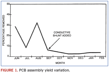
PCB assembly failure rates (Figure 1) were fluctuating between 10 and 30%, and some lots were 100% defective. Production was at a virtual standstill. The cost implications of continued failure were very high and were jeopardizing the entire product line. A detailed failure analysis investigation revealed that virtually all the failures were ESD-induced.
A technical assessment of the manufacturing line was undertaken, and an action plan compiled based on conventional wisdom at the time. Because of the extreme seriousness of this situation, the weekly reports were channeled to high-level executives in the company.
Initially, many extraordinary handling precautions were instituted, such as whole room ionization, bench ionizers, ESD garments, ESD chairs, constant wrist monitors, daily compliance verification, etc. Even with nearly flawless compliance to procedure, yields continued to fluctuate dramatically.
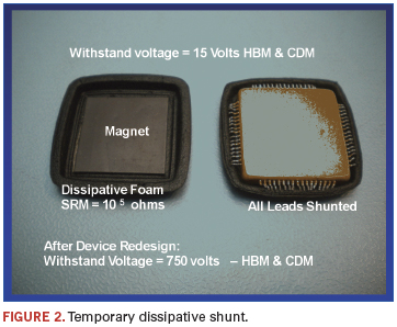
This problem was resolved with the introduction of a customized dissipative shunt referred to as a “top hat” (Figure 2). This shunt consisted of molded static dissipative foam precisely contoured to contact each lead of the device while on the circuit board. The top hat was placed on top of the NMOS device immediately after it had been assembled to the PCB. This resulted in the leads of the device being electrically connected through the static dissipative foam and static potential differences minimized.
The board was then processed normally through the rest of the assembly line until it reached final test, when the top hat had to be removed. This simple addition of a shunt to the device dramatically improved yields and resulted in failure rates of less than 2%.
The simplicity of this solution is particularly striking in contrast to more common alternatives that proved unsuccessful and costly. The extraordinary measures of using a multitude of standard precautions proved to be overkill and ineffective. The solution described here introduces a simple shunt into a set of existing procedures. The incremental cost was merely $1,000 for a set of top hats. The savings realized on the production line reached $6.2 million per year for this one device on this one line and enabled a billion-dollar product line to ship on time.
Another benefit derived was the impact on the design community. Asked to justify a withstand voltage of 20V for the NMOS device involved in the project, designers responded by redesigning the device and raising the level of sensitivity to 750V HBM and CDM, a remarkable accomplishment. Some system–level design changes were made to accommodate the new protection circuitry and maintain system performance.
This case study makes clear that ultrasensitive devices pose a significant threat to production lines and may result in lost production and lost sales. The financial implications are particularly unattractive when the cost of lost sales is added to the cost of lost materials.
As a direct result of the experience outlined in this case study, minimum design requirements were modified and a new set of handling requirements for Class 0 established. It was apparent that a cookbook approach to establishing handling criteria for ultrasensitive devices would not work. For example, it is likely some of the automated equipment used in the assembly process was causing the problem. Clearly, extraordinary controls such as room ionization could not solve the problem. Adding a shunt was not only necessary, but sufficient to protect the device at great economic benefit. In addition, the manufacturing line was able to continue to operate as usual and with minimal disruption.
In conclusion, a number of valuable lessons derived from this experience have led to today’s advanced approaches for Class 0 sensitivities. First, design transfer or new product introduction checklists must include ESD sensitivities, followed by risk assessments for devices below 250V or redesign of the product to eliminate these ultra-sensitive components. Also apparent: Customized solutions are essential for cost-effective mitigation of ESD failures. Advanced auditing techniques available today such as ESD event detection and current probe analysis enable scientific determination of optimal controls and countermeasures. The final ingredient is technical expertise to conduct advanced measurements and to develop application-appropriate remedies. These lessons learned helped to create a foundation for the following case study, as well as the creation of the ESD Journal Class 0 Seal of Approval.
Case study 2: BAE Systems. This case study began during new product introductions, when ESD failures were detected with failure analysis. BAE’s Nashua, NH, site had good ANSI/ESD S20.20 controls in place. However, even one failure would be too many for this high-reliability application. So, prior to ramping up production, BAE decided to bring in external expertise to prevent any production or reliability issues.
The approach started with a baseline technical assessment, followed by customized reengineering of each critical operation, the use of quality tracking metrics and advanced technical training. The detailed process changes involved application-appropriate customization.
The baseline technical assessment is a detailed analysis of each operation, looking at HBM compliance and alignment with ANSI/ESD S20.20. This is followed by advanced auditing techniques that include a variety of ESD event detectors and high-bandwidth current probes. More traditional measurement techniques such as electrostatic voltages can be helpful, but at times insufficient to detect subtle sources of losses. Event detection and current probe measurements have become essential tools for Class 0 applications. They enable systematic modification of each manufacturing operation to be either ESD discharge event free or to exhibit events far smaller than the current failure threshold.
A multi-day workshop was conducted to elevate the users’ understanding of CDM and the technically advanced measurement techniques. Ultimately, the user must be able to fully understand Class 0 mitigation and measurement techniques. This training is reinforced with ongoing technical support for a full year to ensure the level of understanding required to achieve the Class 0 Seal of Approval.
Throughout this process, ESD Quality Metrics, including our novel Yield Risk Benchmarking methodology and meaningful quality metrics, are used to track the improvements. This enables management to set measurable goals and objectives and to efficiently monitor progress.
The benchmarking method is an accurate means of quantifying the performance of an ESD program, and there is a direct correlation to personnel compliance with ESD procedures. It has been successfully applied to hundreds of ESD programs.
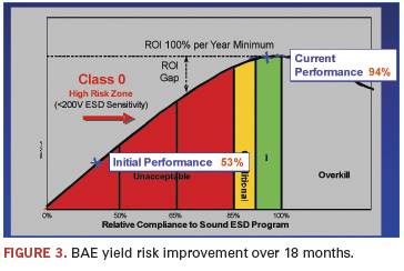
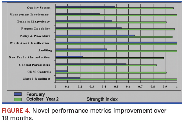
The analysis of the strengths and weaknesses of BAE’s ESD program, as well as the progress over 18 months, is reflected in Figures 3 and 4. These indexes were derived from the novel methodology and were used as a guide for improvement. Virtually all elements now reach 90% or higher. BAE’s Yield Risk Benchmarking score started at 53% and ultimately reached 94%, and its process has not experienced a single ESD failure over a three-year period since implementing Class 0 controls.
Auditing, New Product Introduction and Class 0 Readiness showed sharp improvement. Auditing is one of the more critical elements of program management, and often improvement is essential to mitigate ESD losses. Data derived from auditing can be effective in the early identification and prioritization of process deviations. These data can also be used to effectively leverage limited resources for better Class 0 compliance.
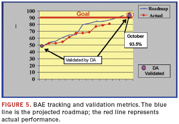
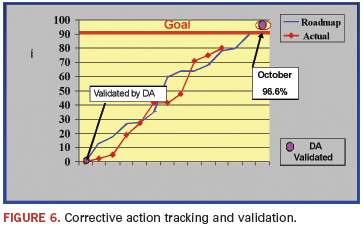
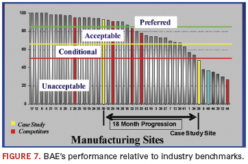
Figures 5 and 6 track improvements. Figure 5 is the novel EPM Yield Risk Benchmarking and is a reflection of the ESD Quality System improvements. The blue line is the roadmap projected at the outset, and the red line is the actual performance that was validated each month. Figure 6 is the closure timeline for the action items in the associated technical assessment. Both trend tracking metrics followed the roadmaps closely, with impressive final scores of 93.6% and 96.6%. Figure 7 illustrates the remarkable improvement relative to the electronics and defense manufacturing industries.
Conclusions
Challenges presented by Class 0 ESD sensitivities are considerable and invariably require customization of mitigation techniques. The strategy employed proved highly effective. ESD failures were virtually eliminated, and the ESD team became competent and prepared for next-generation, sensitive Class 0 devices.
Elements of a good program include the following:
Exceptional program administration, which includes verification of the ESD performance of incoming new product designs.
Quality metrics with tracking scores of over 90% in each category. If you cannot measure an ESD manufacturing process, you do not have a functional process! With the process outlined here, Class 0 products may be successfully produced at very high yields.
CDM and HBM countermeasures to be executed with rigorous compliance verification and virtually flawless adherence to procedure to avoid quality or reliability excursions.
A deep understanding of the ESD technology and Class 0 mitigation techniques, best learned through intense initial training with ongoing reinforcement over a year or more.
CDM mitigation techniques that include both methods: minimizing voltages on the product and controlling the surface resistance of materials that contact the conductive elements of the ESDS product.
Customized reengineering of critical operations and strategic application of dissipative materials and ionization.
Advanced measurements such as ESD event detectors and current probes.
Ted Dangelmayer is president and CEO of Dangelmayer Associates LLC (dangelmayer.com); This email address is being protected from spambots. You need JavaScript enabled to view it..