A Formula for Rebuilding America’s Manufacturing Base and Competitive Electronics Manufacturing Industry
There’s a lot of discussion and speculation today about what’s wrong with the US economy, and what to do about it. It is generally agreed that part of the problem is that America’s manufacturing jobs have been outsourced to cheap labor markets overseas, and that reviving manufacturing in the US, with a healthy export trade, is part of the solution. How to achieve this, though, is the subject of much debate. With price pressure from these foreign markets making American goods less than competitive, how could we succeed?
In the electronics manufacturing industry, a truly global market, US-based manufacturers are in a quandary. The once-robust American electronics manufacturing and assembly industry has been gutted; most consumer electronics are assembled and manufactured in Asia. For example, cellular or wireless phone electronic components are produced almost exclusively in factories in China, Taiwan, Vietnam, and others. But it isn’t merely inexpensive or cheap consumer technology being produced there, but in fact highly complex and sophisticated electronics. This is actually an exception of sorts; generally we assume that high-volume, cheap consumer item manufacture is outsourced, while the lower-volume, more complex or difficult products are produced here. That’s not the case with electronics. Our company, EI, is a printed circuit board fabricator based in the Chicago area. At one time, there was a robust PCB fab industry here in the US, much of it located in Southern California. But now, US-based PC fabricators are less numerous, in large part due to price pressure from overseas and pressure from environmental regulations and compliance requirements. The nature of our industry is such that it involves metals, chemistries, plating baths, and the generation of waste that must be properly treated or disposed of, something that is unfortunately not as much of an issue in countries where such regulations are lax or nonexistent. Compliance, though necessary, is still one factor that impacts cost, which in turn affects price competitiveness with PCBs produced overseas.
In terms of the US manufacturing industry as a whole, there is a way to turn things around. A good example to follow – not easy, but one that has worked – is the model that Germany has developed, sometimes referred to as the “BMW Model.” It must be working; in August of last year, The Observer’s Ruth Sunderland called the bounce-back of German manufacturing “… a testament to a business culture that has respect for manufacturing, and where exporters such as BMW or Bosch do not rely on a cheap currency to sell goods abroad but on the excellence of their products.” Sunderland calls Germany’s so-called Mittelstand – its small and medium-sized firms – “the backbone of the German economy,” adding they have “proved their durability and resilience.”1
And it’s more than that. Germany is a country where the revival of manufacturing is increasingly successful, and as a result they have brought unemployment down sharply to its lowest point in 20 years. Part of the secret has been to keep high-tech, high-capacity manufacturing at home, which keeps quality engineers in the country; they stay because these high-level jobs earn top wages. This keeps the brain trust at home, where it builds products considered the best in quality on the world market. Germany has invested in its people, and works constantly to support technological advancement and keep it in the country. To achieve this, it has continually invested in such things as training and internships, with the goal of keeping skills and knowledge within the country. It also forged successful cooperative associations with universities and educational institutions. The teamwork between government, industry, and institutions of training and higher education was a formula for success in terms of investing in people and providing the tools needed to fill the positions required by demanding technology.
It has been frequently said that America's best industry is producing Ph.Ds and highly educated people, but the problem is that once they have completed their education, they leave. We're losing our brain trust, because the people we educate, often from countries such as China, take that knowledge and return to their homelands, using their new skills to enhance the competitiveness of their domestic industries and economies against the US. In many instances they will help found companies that compete directly with US-based companies where they completed their internships or worked for a year or more!
High-technology, high-end manufacturing jobs pay well and attract the best candidates. They don’t need to be jobs at massive global corporations; in fact, some of the most innovative, forward-thinking, and prosperous companies are the American equivalent of Germany’s Mittelstand: small or mid-sized, established firms that invest in development and innovation. We need to invest in people – knowledge and training – and orient our efforts more toward those industries that demand a high level of knowledge and competence. Currently, we use only 22% of our total economic capacity here in the US for manufacturing; we are primarily a service sector economy. We can’t grow the US economy based solely on service. The German model is a bit different, where about 30% of the economy is industry and 70% is in the service sector. Remarkably, this is only about a 10 percentage point disparity, but in practice it constitutes a world of difference. Judging by the German model, if we shift only 10 percentage points of our resource capacity into manufacturing, perhaps a little more, we can go a long way to turning around the economy within a decade or two. Remember that economic growth is based on the GDP. The GDP in turn is based on earnings. High tech jobs require greater skills and training, and as a consequence, those jobs command better rates of pay. This contributes to boosting the GDP.
American industry has an ace in the hole, so to speak, that can help this turnaround, and also serves as an argument against outsourcing, and that is US infrastructure, manufacturing and transportation. Many people considering outsourcing don’t realize all the costs involved in sending work overseas. More than merely the costs of shipping, there are costs associated with lost time and risk factors that only become apparent once the process has begun. Developments in US infrastructure, begun during the Eisenhower years, have made the US the most cost-effective and reliable place to manufacture and deliver product. The logistics system within this country’s infrastructure is very efficient. Transportation in the US is still more efficient and cost-effective than anywhere else in the world. The lower risk factor associated with shipping goods within the US is a major cost consideration and incentive for manufacturing here.
Earlier we mentioned how high-volume, inexpensive consumer products for many industries are outsourced for manufacture in China, for example, while many high-reliability products continue to be manufactured here – in many cases. Yet, in the printed circuit board and electronics sector, this formula has been turned on its head. More complex printed circuit boards are being made overseas and shipped here for assembly, while low-tech circuitry, the type of technology that is been around for 20 years and more, is being produced here in the United States – the country that invented PCB technology! In fact, the majority of complex printed circuit boards assembled in the US are fabricated in Taiwan and China. The recipe for success for American electronics is to reverse this trend, so that the low-tech boards are being produced overseas, and the highly complex circuit assemblies and boards are being manufactured and fabricated here in America. It sounds like a simple solution, but it is not an easy one to implement; in PCB fab, for example, price pressure from overseas is high and margins are slim. It will take better machines, better technology, and more skilled engineers to boost the capability – not capacity – of electronics manufacturers here. That’s investment – and where is it to come from? If a US PCB fabricator can invest in greater capability; e.g., smaller features, lines, and connections on PCBs, to compete with overseas suppliers, we can resume advancing technology here and compete globally, sinking money into innovation and technology development.
Banks and finance institutions will need to provide needed financial support, such as low-interest loans, so they can invest in new equipment and move up to the next level of development. But I suggest this would take five or six years minimum. We know the recipe, but we don't quite know how to get there. We need a roadmap, and the roadmap begins with some sort of financial support to promote development in the circuit board industry, so that we can bring higher technology manufacturing back to the US to support growth and jobs. If these PCB manufacturers can expand their capabilities, the growth will follow and high-tech American products will be sold competitively in the world market.
There is a ripple-effect benefit as well. Electronics contract manufacturers and assemblers, also known as EMS providers, will grow too, and be more competitive, because they will have more local sources for boards for more complex products. The ripple effect will be felt across many associated industries, and have a direct benefit on the national economy. Too many US-based EMS companies buy their bare boards from overseas because fabricators in the US do not offer many products or even the capacity or capability to provide them.
We should focus on doing what we need to make our economy more lean, more efficient, more productive, and more complex, with a greater range and diversity of manufacturing. This will begin to reverse the tide of outsourcing and thereby grow the national economy while we enhance the prospects for our own businesses.
References 1. Ruth Sunderland, “German Business Culture Should Be a Model for Our Own,” The Observer, Aug. 14, 2010.
Pratish Patel is president and CEO of Electronic Interconnect (EI).
Putting these two under one roof provides OEMs greater assurances the end-product is successfully tested and avoids unforeseen problems.
PCB layout and test are inextricably intertwined. Some contract manufacturers maintain an in-house staff of layout designers, as well as assembly/test engineers. In such cases, the layout engineer delays creating all the necessary test points to avoid hindering routing. But once they finish critical routing and bus routing, an initial routing analysis and preliminary test points to achieve, say 50 or 60% coverage, they have the benefit of consulting with in-house test engineering to determine the right strategy to increase test coverage for the product.
OEMs that fail to take advantage of this basic and important practice when mapping out their system designs and manufacturing incur the greatest potential for extra costs, wasted time, and latent field failures. Consider the OEM that hands its printed circuit board design to a vendor located in one sector of the country. Then that OEM sends the electronic data (Gerber) to a fabricator at another geographic location. Afterward, the OEM purchases components and locates a third-party to perform assembly. Each stage – design, fab, and assembly – is distinctly separate from the others and, in effect, operates within its own confines with the OEM trying to successfully orchestrate the entire production cycle.
This process doesn’t make much business sense anymore, other than perhaps trying to save a few extra dollars. However, some OEMs still do this, especially those serving medical device and mil/aero markets, in which the slightest glitch can cause catastrophic consequences. Surprisingly, the consensus stance for doing it this way is simply, “We always have.”
What can go awry when opting for disparate operations? The OEM’s timeline, for starters. Consider the layout engineer at a selected PCB design house that performs only design and layout. Quite likely, they are involved with several design projects, each with specific completion dates. If that PCB layout engineer is behind schedule, causing a design to be late in delivering it to the fabricators, that triggers a domino effect with the fabricator experiencing unexpected delays, and delivery to the assembler (and market) gets compounded.
Murphy’s Law plays a role. Bad things do happen. The design and fabrication processes don’t quite jibe. The deliverables are not complete, or some critical information is missing, such as drill chart callouts or impedance control information. But the layout house argues that the problem rests with the fabricator. Finger-pointing continues until the problem is resolved, after much wasted time. Also, when using uncoordinated fabrication and assembly operations, the OEM fails to gain the benefits of highly coordinated resource expertise, which can be the difference between a product’s success and its failure.
Layout and Test Collaboration
Aside from these adverse issues, the crucial step of testing often gets short shrift when layout and assembly/test are vastly and geographically distant from one another. Ideally, a product gets the highest testing coverage possible – in the area of 85 to 95%. To accomplish those goals, having test and layout engineering under the same roof offers greater assurances they interact and jointly devise plans to successfully test the end-product. Experienced test engineers know all the nuances associated with in-house test systems. This is valuable knowledge that test engineers and technicians can pass to in-house layout engineering to be factored into designs.
It also helps when a seasoned layout engineer is familiar with flying probe and ICT test guidelines and limitations. For example, when a flying probe cannot reach a specific part of the board, that portion cannot be tested, thus reducing the test coverage. Then the layout engineer, keeping in mind those testing guidelines, can generate either more test points or use vias as test points to overcome that tester limitation (sidebar).
Testing is not jeopardized or shortchanged when PCB layout and test engineering maintain steady, orderly and productive collaboration. When a layout enters its final stages, the layout designer can transfer the CAD layout data to the testing department, where the testing access reporting mechanism can discern how much test coverage is actually available and on which kind of tester, keeping in mind the tester limitations. Here is where layout and test interaction pays handsome dividends. At this point, a series of mini conferences take place to discuss the steps the layout engineer needs to take to increase test coverage. Say, for example, test engineering determines a nearly completed design exhibits only 60% coverage. Since the PCB is still in the layout phase, the designer can use the new details and suggestions to add more test points or test vias, thus increasing testability access.
In this role, the PCB layout engineer must step out of their traditional design engineering routine and embrace a variety of test-related practices, procedures and disciplines, which need to be folded into the layout strategy at the placement, routing and finishing stages for a given board design. A classic example involves decoupling capacitors tied to an IC’s VCC or power pin. The smart PCB layout engineer ensures even distribution of those decoupling capacitors to help reduce noise. If the IC is not decoupled properly, locally generated noise ripples through the entire circuitry, creating jitter and ringing effects on the board. Those effects are later caught at the test stage, and the layout needs to be changed to reduce noise and jitter.
In another instance, the layout engineer must pay special attention when designing a high-speed bus that requires improved impedance and coupling control to satisfy the circuitry’s voltage and timing budgets. Special layout emphasis is critical for the bus design’s geometry and traces to develop proper test coupons. If not done properly, timing budgets will be off, and those mistakes will be caught at either debug or functional test stages, effectively too late for changes, short of re-spinning the board.
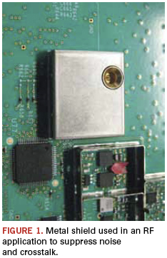
Also, in an RF application, signals generate parasitic coupling. The PCB layout engineer must implement ground shields or floods at the right locations in the layout to reduce parasitic coupling (Figure 1). Improving trace-to-trace impedance control is achieved by inserting ground shields between signal lines. This improves a uniform copper density across the entire board to ensure etch characteristics are equal to all signal lines. Again, if that’s not properly performed, test results send the layout back to the design for another go around.
Those are a few examples of what the savvy PCB layout engineer must know to successfully prepare a layout to achieve high-test coverage. Further, it’s important they fully understand the significance of such test procedures and characteristics as smoke test, gain and frequency response test, analog signature analysis (ASA), propagation velocity test, probing techniques, launch edge versus reflection edge, filtered TDR option, and others.
The smoke test is conducted to ascertain that data or signal aspects of the board are properly functioning. There are differences between a smoke test for digital and analog components. A smoke test provides some necessary assurances that system-under-test will not catastrophically fail. In other words, the circuit will not burn or systems will not crash. An example of the smoke test is the gain and frequency response testing. This involves measuring resistive points or loads between two different points to ensure they are balanced. The PCB layout engineer must understand this test because it helps prevent the circuit from burning, or at least avoids big mistakes from happening.
ASA monitors jitter, which occurs in digital ICs where the solid state jumps between two or three different points, thus causing instability. The experienced layout engineer will ensure a propagation delay between those two traces in order to make a stable state for doing ASA analysis, to control the jitter, and to ensure it’s within allowable parameters.
Propagation velocity testing involves propagation delay measurement and impedance measuring. Controlling impedance is relatively easy, and performing calculations and controlling a few factors to achieve impedance control is not difficult. But measuring propagation delay is considerably more difficult. Accuracy is extremely dependent on probing techniques dealing with connecting and terminating leads. Among the ones the PCB layout engineer needs to know about are handheld devices, SMA connectors, and controlled impedance micro probes, so they can factor in these test tools and considerations during layout.
As for launch edge versus reflection edge, the PCB layout engineer should have a firm understanding of this characteristic when doing high-speed designs. Last, filtered time domain reflects (TDR) option is used when excessive ringing occurs on a TDR response. Rise and fall edges must be aligned so they have zero time delay between rise and fall. Having this knowledge, the layout engineer is able to design the circuitry that is stable and has no jitters.
Sidebar:
Key ICT Guidelines
Don’t tie IC control lines directly to power or ground. Add pull-up or pull-down resistors. This permits the ICT to control these lines when required during IC testing.
Place test points away from BGA components to reduce BGA solder stress and board flex.
Have a test point for all electrical nodes, including unused IC pins. This allows detection of internal and external shorts.
To measure a low ohm resistor, two test points on each side of the component may be required to support 4-wire Kelvin resistance measuring.
Oscillator should be gated with logic circuit, allowing ICT to disable the clock signal as needed during IC testing.
Use boundary-scan-compliant devices when possible. This provides accessibility to the devices for boards with limited access test points. Also, chain multiple JTAG devices.
If possible, place test points for each node on one side of the board (secondary side preferred). This reduces the fixture and maintenance cost. Top-side probing is less accurate than bottom-side probing.
Zulki Khan is founder and president of NexLogic Technologies (nexlogic.com); This email address is being protected from spambots. You need JavaScript enabled to view it..
Written by Srinivas Durgam, Chandran Achutan, Ph.D., Carlos Aristeguieta, M.D., and Maureen T. Niemeier
Category: 2011 Issues
A review of best-in-class controls for maintaining factory worker health.
The National Institute for Occupational Safety and Health (NIOSH) received a confidential employee request for a Health Hazard Evaluation (HHE) at an electronics manufacturer specializing in printed circuit board fabrication, assembly, and testing for different end-user applications (sidebar). At the time of our evaluation, approximately 2,300 employees worked at the facility in either the medical section plant or the defense and aerospace section. Employees were primarily concerned about exposure to solder paste and fumes, as well as dust and noise. They reported coughs, burning eyes, nosebleeds, voice loss, headaches, sinus infections, bronchitis, and respiratory problems.
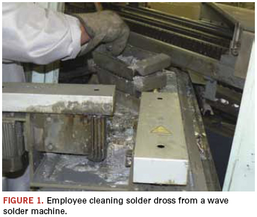
At the time of our evaluation, the medical section had four wave soldering lines and eight surface mount lines. Wave solder lines 1, 2, and 3 used Pb-free solder (96.5% tin), and wave solder line 4 used solder composed of 63% tin and 37% lead. The defense and aerospace section had five wave solder lines and six surface mount lines. It also had ruggedization, conformal coating and bonding operations, where the finished PCBs are fitted with additional structural supports and hand-brushed or sprayed with an acrylic copolymer to provide increased environmental and mechanical protection. Spraying during conformal coating was conducted in a ventilated, open-face, bench-top spray booth. Employees wore safety glasses and air-purifying, elastomeric, half facepiece respirators with organic vapor cartridges while spraying. At least once per shift, wave solder operators clean solder dross by using a ladle to remove dross floating on top of the molten solder (Figure 1). Residual molten solder inadvertently collected during this operation is separated with a sieve, and the remaining dross disposed of in a drum sealed with a lid. Employees are required to wear heat-resistant gloves over disposable nitrile gloves, a face shield, and an apron when performing dross cleaning. In addition to dross cleaning, employees periodically clean and maintain the wave solder machines. Finally, the facility has an auto insertion (AI) operation, which involves machine insertion of components onto a PCB by punching through it.
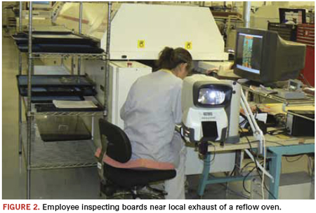
Assessment. During our first visit to the facility, we conducted confidential medical interviews with 40 employees, observed work processes and practices, collected general area air samples for volatile organic compounds (VOCs), and collected surface wipe samples for lead and tin. We also reviewed air sampling records, the respiratory protection program, injury and illness records, and material safety data sheets. After sharing our findings with employee and management representatives in an interim letter, we returned to the facility to collect personal breathing zone and general area air samples for lead and specific VOCs. We also measured noise levels at the AI stations, evaluated room acoustics near the air rotation units (ARUs), collected hand wipe samples to assess lead contamination on skin, and evaluated the effectiveness of the local exhaust hoods for the wave solder and surface mount machines (Figure 2).
Occupational exposure limits. NIOSH investigators use both mandatory (legally enforceable) and recommended occupational exposure limits (OELs) for chemical, physical, and biological agents as a guide for making recommendations. OELs have been developed by Federal agencies and safety and health organizations to prevent the occurrence of adverse health effects from workplace exposures. They suggest levels of exposure to which most employees may be exposed up to 10 hr. per day, 40 hr. per week for a working lifetime without experiencing adverse health effects. However, a small percentage of employees may still experience health effects due to personal susceptibility, a preexisting medical condition, and/or hypersensitivity (allergy). In addition, some hazardous substances may act in combination with other workplace exposures, the environment, or with medications or personal habits of the employee to produce health effects, even if occupational exposures are controlled at the level set by the exposure limit. Also, some substances can be absorbed by direct contact with the skin and mucous membranes in addition to being inhaled, which contributes to the individual’s overall exposure.
Results and Discussion
One of six personal breathing zone air samples for lead exceeded the Occupational Safety and Health Administration action limit (OSHA AL) of 30 micrograms per cubic meter (µg/m3) and was close to the OSHA permissible exposure limit of 50 µg/m3. This employee, a wave solder operator in the DAS, was cleaning the wave solder machines without wearing a respirator. The employee was exposed to an airborne lead concentration of 49 µg/m3. However, with this one exception, wave solder operators had lead exposures well below the OSHA AL.
Our surface sampling showed the presence of lead and tin on work surfaces in both sections of the plant. Currently, there are no OELs for surface metal contamination in occupational settings. We also sampled tables in two of the break rooms and found detectable levels of lead and tin in one of the break rooms. This suggests that workplace contamination is being tracked into the break rooms by employees’ footwear, clothing or hands, and that these areas should be kept cleaner.
Additionally, despite hand washing prior to sample collection, three of seven hand wipe samples tested positive for lead.
Full-shift noise exposures for the AI operators in the medical and defense and aerospace section were well below the NIOSH recommended exposure limit. Because telephone communication is not required in the production areas, and communication between employees is minimal, the louder noise levels experienced by employees with work stations near the ARUs were within the criteria specified by the balanced noise criteria (NCB) 55-70 curves. The NCB curves are a set of noise criteria for occupied interior spaces, devised to limit noise to levels at which speech can be reasonably understood. Refer to “Resources and Links” for more information on the NCB curves, as well as Appendix B of the HHE report (referenced in this section).
Our ventilation evaluation revealed that several local exhaust hoods were not effectively capturing process emissions. These included three hoods in the medical section and two hoods in the defense and aerospace section. This could have been due to local exhaust ventilation systems being imbalanced or improperly maintained. Air sampling results for specific VOCs indicated that employee exposures were well below all applicable OELs.
Although both the medical and defense and aerospace section share the main workspace and have similar tasks and equipment, the health concerns originated exclusively from employees in the medical section. Of the 40 medical section employees we interviewed, 23 did not report any work-related symptoms. The most commonly reported symptoms were upper respiratory, including runny nose, cough, and sinusitis; fatigue (frequently related to overtime work), and voice loss. However, these symptoms are also common in the general population, and we could not attribute them to the exposures documented.
Last, we found inconsistencies between the facility’s written respiratory protection program and employee practice. The written respiratory protection program required respirators to be worn when cleaning wave solder machines. However, it did not identify the appropriate type of respirator that should be worn for this task, and we did not observe employees wearing respirators when performing this activity. In addition, employees were voluntarily wearing respirators during spraying in the conformal coating area.
Recommendations
We made a number of recommendations to the facility to improve employee health and safety. Many of these recommendations may also apply to readers’ facilities:
Use engineering controls such as portable exhaust hoods when removing solder dross and cleaning wave solder machines. Periodically evaluate the local exhaust hoods to ensure they are performing per manufacturer’s specifications. Evaluate their effectiveness at least every three months, and within five days of a production, process, or control change.
Comply with all requirements of the OSHA lead standard (29 CFR 1910.1025). This includes instituting an industrial hygiene monitoring program to assess lead exposure for employees working with leaded solder, or for employees having the greatest potential for lead exposure. Additionally, institute a maintenance program for evaluating enclosed local exhaust hoods used to control lead exposure.
Improve general housekeeping practices to ensure break rooms and work surfaces are clean. Use commercial cleaning wipes that are made for removing lead and other heavy metals every shift to keep work surfaces such as control consoles clean. Use high-efficiency particulate air vacuum cleaners in work areas to minimize dust in the air.
Practice good personal hygiene. Thoroughly wash hands before eating, before and after using the restroom, and before leaving work. Eating, drinking, smoking, and applying cosmetics in work areas should be prohibited.
Ensure that the respiratory protection program meets all applicable requirements of the OSHA Respiratory Standard (29 CFR 1910.134). The written respiratory protection program should identify job tasks requiring a respirator to be worn, the type of respirator needed, and the locations where respirator use is required. Evaluate respiratory hazards for job tasks currently requiring respiratory protection to ensure protection is adequate. The program should also note any job tasks for which employees voluntarily wear respirators.
Encourage employees to report work-related health concerns. Consult a physician trained in occupational medicine (see “Resources and Links”).
Train employees about potential exposures and how to protect themselves from hazards, and promptly communicate any health and safety changes to employees.
Sidebar:
The Health Hazard Evaluation Program
Based on a federal law, NIOSH conducts Health Hazard Evaluations (HHE) to investigate possible workplace health hazards. Employees, employers or union representatives can ask our comprehensive team of experts to investigate their health and safety concerns by requesting an HHE. Our team contacts the requestor and discusses the problems and how to solve them. This may result in sending the requestor information, referring the requestor to a more appropriate agency, or making a site visit, which may include environmental sampling and medical testing. If we make a site visit, we prepare a report of our investigation that includes recommendations specific to the problems found, as well as general guidance for following good occupational health practices. HHE reports are available on the Internet (http://www.cdc.gov/niosh/hhe/).
Resources and Links
1. NIOSH HHE program information, cdc.gov/niosh/hhe/HHEprogram.html. 2. Link to this HHE report: cdc.gov/niosh/hhe/reports/pdfs/2007-0201-3086.pdf. 3. Code of Federal Regulations (CFR), 29 CFR 1910.95, US Government Printing Office, Office of the Federal Register. 4. L.L. Beranek, “Criteria for Noise and Vibration in Communities, Buildings, and Vehicles,” Noise and Vibration Control, Rev. ed. Cambridge, MA: Institute of Noise Control Engineering; 1988:554-623. 5. L.L. Beranek, “Balanced Noise Criterion (NCB) Curves,” J Acoust Soc Am., 1989; 86(2):650-664. 6. Acoustical Society of America, ANSI S12.2-1995, “Criteria for Evaluating Room Noise,” 1995. 7. Association of Occupational and Environmental Clinics (aoec.org). 8. American College of Occupational and Environmental Medicine (acoem.org).
Srinivas Durgam was an industrial hygienist at NIOSH (cdc.gov/niosh) during the time of this evaluation; This email address is being protected from spambots. You need JavaScript enabled to view it.. Chandran Achutan, Ph.D., is assistant professor at the University of Nebraska Medical Center (unmc.edu); This email address is being protected from spambots. You need JavaScript enabled to view it.. Carlos Aristeguieta, M.D., was a NIOSH medical officer during the time of this evaluation; This email address is being protected from spambots. You need JavaScript enabled to view it.. Maureen Niemeier is a freelance technical writer; This email address is being protected from spambots. You need JavaScript enabled to view it..
Every dimension poses a risk to yields or time. Make sure they are worth it.
This month’s question: What is the typical industry standard for tolerance on the length and width of a flex circuit and also for stiffeners?
Answer: When it comes to dimensioning and tolerancing flexible circuits, less is usually better. Too many designers try to dimension a flex circuit as if it were a machined piece of steel. Keep in mind that the materials used to fabricate a flexible circuit are flexible. In addition to standard manufacturing tolerances, factor in the flexibility and dimension instability of the materials used in the construction.
A lot of factors cause flex circuit materials to grow or shrink before, during and after the circuit is constructed. Major physical factors that contribute to the dimensional instability of a flexible circuit are temperature and humidity. Like any material, polyimide film and acrylic/epoxy film adhesive (by far the most common building blocks for a flexible circuit) will expand when heated and shrink when cooled. While these changes may be small, over many inches of circuit length, they can add up. The other culprit is humidity. Flexible circuit materials are extremely hygroscopic and will not saturate until they have absorbed nearly 3% of their weight in moisture. As the circuits absorb moisture, they expand. The combination of temperature and humidity can cause a flex to change up to 0.001" per inch of length. So you can see that putting +/-0.005" on a 12"-long circuit can cause some problems.
Many years ago, I had a customer who ordered 18"-long flex circuits that had a tolerance of +/-0.005" on the overall length. Being young and inexperienced (I wasn’t always a Flexpert), I missed this, and we built and shipped the parts. About a week or so later, I received a call from the customer’s QA engineer telling me that the circuits were averaging 0.004" out of tolerance on the long side. I had the parts shipped back and when I measured them, they were actually averaging 0.001" under nominal. To make a long story short, these parts achieved frequent flyer status as they went back and forth between our facility and the customer’s. After about the third round, I realized what was happening. We were building the circuits in January in Minnesota (i.e., -20°F outside and less than 10% humidity inside). The customer, on the other hand, was in Tampa Bay, FL, where there is nearly always a fair amount of moisture in the air. All along, the parts had been growing and shrinking due to the wide variation of humidity levels between the two locations. I asked the customer’s QA engineer to give the circuits a low temp bake for an hour or so, and then measure them immediately after they cooled. Bingo! He got the same measurements as I was.
The bigger question is why had they specified +/-0.005" on a flex circuit 18" long? Did I mention that flexible circuits are flexible? I can’t imagine what application would need a tolerance that tight on a flex that long.
On the vast majority of drawings, I prefer to see just a few overall length and width dimensions that are reference, and let the CAD data drive the rest. If there is a dimension that is truly critical, by all means put in on the drawing and tolerance it accordingly. But realistically, since a flex circuit can bend, twist and flex, very few dimensions are truly critical. All dimensions on a drawing will have to be verified, which will add cost to the circuit. The designer needs to evaluate all dimensions that they put on the drawing and ask themselves if that dimension is going to add value, or just add cost.
So to answer the original question: Length and width of FPC would be +/-0.010" plus 0.001"/inch of length. This is the tightest that I would ever agree to, and I would prefer +/-0.020" plus 0.001"/inch.
Length and width of stiffeners. Since stiffeners are machined and constructed from a much more dimensionally stable material, they can hold tighter tolerances. But since you are putting them on a part that cannot support tight tolerances, are tight tolerances on a stiffener really necessary? They usually are not. For most normal-sized stiffeners, +/-0.010" is usually safe.
Always keep in mind that you pay for every dimension on a drawing either directly by potentially causing lower manufacturer yields or indirectly by requiring the manufacturer to verify each dimension. When dimensioning a new design, ask yourself if all those dimensions are adding value. Are you getting your money’s worth?
Mark Finstad is a senior application engineer at Flexible Circuit Technologies (flexiblecircuit.com); This email address is being protected from spambots. You need JavaScript enabled to view it.. He and co-“Flexpert” Mark Verbrugge from PICA Manufacturing Solutions (This email address is being protected from spambots. You need JavaScript enabled to view it.) welcome your questions.
“Design by plug-in” comes to printed circuit board CAD tools.
Have you ever wished for a feature in your design tools, maybe even requested it from your EDA vendor, but never seem to get what you want? I hear that a lot from my customers, and I doubt I’m alone. Sometimes the requests are good ideas that everyone can use, and they make the development list. Sometimes the requests facilitate a custom flow or procedure that just isn’t appropriate for a shrink-wrapped product. Regardless of how the request is categorized, it always seems to take longer to implement than the customer would like, mainly because they’d really like it right now.
Contrast this situation with your iPhone, iPad, or Droid phone. Need some new functionality? Chances are someone has already thought about it and created an app for it. I am amazed at the abundance of apps out there for smartphones and pads. Need a scientific calculator app? It’s there. How about an alarm clock, a gas mileage manager, voice recorder, book reader, or even the Angry Birds game? They’re all available.
Wouldn’t it be nice if you could get those apps in your design tool? OK, maybe not, but I would bet you can think of a lot of more germane nice-to-haves. I had one customer ask for a feature to synchronize test point placement between their PCB and schematic. Another said it was too difficult to find specific parts or values in their library of designs, and couldn’t we make that easier? Yet another wanted to automatically add various visual cues relating to production status to their schematic. There’s a never-ending stream of wants and desires out there. Sounds like the perfect scenario for a healthy dose of apps.
As PCD&F reported earlier this year, Cadence got things started by adding an app store to its OrCAD Capture frontend tool. Remember those customer requests I just mentioned? We implemented them for the customer, and then made them more generic for the general population and released them as apps. Apparently this isn’t unique to us, as other VARs are doing the same thing, helping us to create the first app store for the PCB design community.
We showed the apps and the store at the recent PCB West trade show, and found that users were thrilled to see that they had a new way to get more capabilities that they need, and that they could pick and choose which ones to get. As excited as I am to get this kind of response, I was probably more excited to hear other users saying they had some ideas and wanted to know how they could create their own apps. Imagine that: PCB tool users creating solutions to solve their own problems and then adding them to the pool of apps available to everyone.
This is similar to the concept of open source in that the user community has the ability to continually improve the tools they use. However, with apps, the added capabilities plug into the tool rather than modifying its base, so these new features become available the moment they are finished, rather than at the next release of the base tool. Another difference is that apps are based on scripting languages that are simpler to learn and use than C++ or many of the other programming languages used to create PCB tools. The developer has access to the database, command structure, and menu structure, making it relatively easy to implement features. Finally, problematic apps don’t ruin the whole tool; they can simply be removed.
That brings up a vital part of an app community: separating the good apps from the bad. Anyone actively downloading apps on their handheld devices knows that there are a lot of duds out there. Some just plain don’t work as advertised. We’ve built in quality assurance measures to minimize this problem, but the truth is there will still be imperfect apps. The key to this problem is the familiar rating system. Users of the apps get to rate the apps. Good apps get good ratings, and bad apps get left behind. It can be harsh, but it’s necessary to let this Darwinian approach to apps weed out the undesirable ones.
Another nice use of apps is to integrate existing tools with the schematic or PCB editing tool. We’ve come to expect the ability to launch another tool from the same vendor, but wouldn’t it be nice to build bridges between different vendors’ tools, especially if that bridge includes built-in knowledge of design? Similarly, a company with internal tools can create a more effective flow by tying the tools together. These apps can plug in to different versions of the PCB tools and can be shared between different design teams or the community at large.
I can see the user community adding some real vibrancy to our industry. It’s not too hard to imagine many apps available, because we’ve seen this with smartphones and pads, but I can also see a pool of developers looking for good ideas to implement. Some in the community will implement what they need with the scripting language, but others will take their wants and desires to an app developer for much quicker results, conforming to their specific needs. In fact, I’ll sign up to host the first app developer request line. Send me your wants and desires, and we’ll get to work building an abundance of PCB design apps.
Manny Marcano is president and CEO of EMA Design Automation (ema-eda.com); This email address is being protected from spambots. You need JavaScript enabled to view it.. His column runs regularly.
No panacea exists, but certain coatings are getting closer.
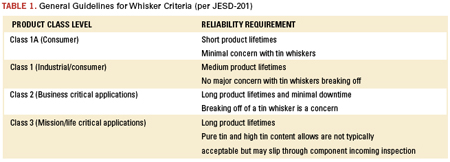
What are the guidelines for tin whiskers in electronics assemblies, and how are they prevented? Part of the question can be answered by the Jedec and GEIA standards that delineate acceptance requirements for tin whiskers (Figure 1) in commercial and military hardware. But none of the methods outlined by the standards guarantees total mitigation of whisker growth.
No single accepted theory explains the tin whisker growth mechanism. The leading theories postulate the growth mechanism is powered by a release of internal stress in the tin finish or by re-crystallization and abnormal growth in the tin grain structure.1 Since the growth mechanism is not fully understood, the required environmental stress tests used for qualification, such as thermal cycling and thermal aging, do not necessarily simulate tin whisker growth in an assembly. A linear growth rate for tin whiskers has not been observed during long-term studies of whisker growth. There is a latency period after the coating is applied during which tin whiskers do not grow, which can range from a period of days to years. Once a whisker starts growing, it will most likely grow at a constant linear rate, but not all whiskers on a particular finish will grow at the same rate. This unpredictable whisker growth rate, which leads to inaccurate acceleration models, makes qualification testing of high-reliability electronics assemblies a challenge.
Qualification tests. For tin whisker acceptance testing, the commercial electronics industry has used Jedec standard JESD201, Environmental Acceptance Requirements for Tin Whisker Susceptibility of Tin and Tin Alloy Surface Finishes. Due to the long service life (>10 years) required for high-reliability electronics assemblies used in the aerospace and defense (A&D) industry (Table 1, Class 3), JESD201 requirements are not adequate. While valuable as a process evaluation tool for data comparison, the environmental test conditions do not correspond with actual A&D service environments. Tin whisker testing in JESD201 focuses on humidity, thermal cycling (1,500 cycles maximum), and calendar aging for a maximum of only 4,000 hr. (5.5 months). The A&D environment includes vibration, shock, corrosion, and even probe marks in the surface finish left behind during troubleshooting. These environmental conditions induce stress on the thin tin finish, which promotes the growth of tin whiskers.
GEIA-STD-0005-2, Mitigating the Effects of Tin Whiskers in Aerospace and High Performance Electronic Systems, is presently the adopted standard used to manage (but not eliminate) tin whisker risk. These mitigation methods include SnPb solder dipping of component leads, conductor spacing control, and conformal coating. Unfortunately, the current knowledge base does not include decades of experience to verify the success of these mitigation methods and their effect on system reliability.
Mitigation techniques. While pure tin and high tin content finishes are not recommended for Class 3 assemblies, the push to restrain A&D electronics costs has precipitated the use of COTS (commercial off-the-shelf) components whenever possible. Unfortunately, since pure tin finished devices are common and inexpensive, they have inadvertently made their way through A&D supply chains. Component manufacturers and distributors frequently use the lot number as the only discriminator to distinguish the Pb-free finish. Even reputable distributors have difficulty tracking lots of pure tin finished components versus the same component with an alternate finish.
As a first level of tin whisker mitigation, it is critical to screen for pure tin finished components at incoming receiving. Conformal coating, required for most military applications, is another whisker mitigation technique frequently used to help retard the effects of whisker growth. By isolating individual leads, the coating can prevent arcing due to whisker bridges. The more elastic coatings rely on elongation properties to prevent penetration. Other coatings rely on their hardness to restrain or redirect whiskers to grow back on themselves, preventing them from breaking through and potentially shorting. It must be reiterated that currently conformal coating is not a foolproof method to prevent whisker growth.
Various methods and materials are available for conformal coating. The following have been the most commonly used, with most having been qualified under IPC-CC-830. The coatings are listed in increasing order by their expected tin whisker mitigating value.
1. Acrylic: can be dipped or sprayed. 2. Silicone: can be dipped or sprayed. 3. Epoxy: can be dipped or sprayed. 4. Parylene: chemical vapor deposition. 5. Arathane 5750 (formerly Uralane 5750)2 Urethane: can be dipped or sprayed. 6. ALD-Cap3: high alumina ceramic applied using atomic layer deposition.
With research still pending, ALD-Cap high alumina conformal coating has shown encouraging signs as a reliable method for tin whisker mitigation.
References
1. Jay Brusse, Kim Jong, Michael Sampson and Henning Leidecker. “Basic Info on Tin Whiskers.” NASA Electronic Parts and Packaging (NEPP) Program, http://nepp.nasa.gov/whisker/background/index.htm. 2. Jay Brusse, Kim Jong, Michael Sampson and Henning Leidecker, “Characterize the Effectiveness of Arathane 5750 (formerly Known as Uralane 5750) Conformal Coat Material in Prohibiting Tin Whisker Formation and/or Tin Whisker Penetration.” NASA Electronic Parts and Packaging (NEPP) Program, http://nepp.nasa.gov/WHISKER/experiment/exp2/. 3. Ofer Sneh, “N04-058: ALD-Cap: Thin Film Encapsulating Coating for Hermetic Environmental Protection,” Navy SBIR Success Story, July 25, 2009. https://www.navysbirsearch.com/widgets/hyperlinking/successdetails.jsp?url=DocURL&id=90078. 4. The Lead-Free Electronics Manhattan Project – Phase I. Benchmarking and Best Practices, July 30, 2009. http://www.dodb2pcoe.org/LFEMP_book.pdf.
ACI Technologies Inc. (aciusa.org) is the National Center of Excellence in Electronics Manufacturing, specializing in manufacturing services, IPC standards and manufacturing training, failure analysis and other analytical services. This column appears monthly.