IMAPS’ latest workshop showed just how far wafer-level packages have come.
Mobile phone shipments will account for more than 1.6 billion units this year, led by smartphones. The industry also is seeing a major shift to tablets for computing, communications, and many functions no one dreamed of a few years ago. With growth in these products and consumer preferences for thin, lightweight electronics comes demand for thin packages.
It was against this backdrop that IMAPS held its first Advanced Technology workshop on thin IC packaging in Santa Clara, CA, at the end of August. The following is a recap of the workshop.
Substrate warpage has proved challenging for packages, as substrate body sizes increase and thickness decreases. This has been especially critical in package-on-package (PoP). Three major IC package assembly subcontractors – Amkor, ASE and STATS ChipPAC – discussed PoP developments and issues, providing insight into the future of these packages. Shinko Electric provided details of its new embedded die technology, in which active die are embedded in the substrate of the bottom package in the PoP, enabling a lower profile package. ASE discussed its embedded chip process, in which the die is embedded in a buildup structure using laser drilling and metallization of microvias using an electrically conductive epoxy. Results from embedded die research programs at Georgia Tech were also presented. Amkor discussed the effects of package pitch and thickness reduction on board level reliability, as well as thermal fatigue issues for wafer level packages and flip chip CSPs. Hitachi Chemical introduced its new low CTE materials. Panasonic Electric Works discussed its substrate core material and new molding compounds. ASE provided details of its thin substrate. The 90µm thick a-S3, a prepreg glass fiber reinforced construction, is a single-sided substrate with al routing in one plane. Ajinomoto updated attendees with a preview of its next-generation buildup materials.
Recognizing the importance of materials in achieving thin packaging, several presentations focused on key technologies and breakthroughs in material development. With Amkor revealing further details of its copper pillar process, the importance of understanding the interaction between various materials could clearly be seen. In explaining that controlling mold shrinkage is critical, Panasonic Electric Works noted materials for next-generation flip chip CSPs with smaller gaps, adding that the molding materials would require smaller filler particles. Henkel presented developments in conductive die-attach film adhesives and wafer backside coating materials. Also introduced were new underfill materials from Henkel such as nonconductive paste (NCP) and wafer-applied underfill, both of which can be used with copper pillar bumps and TSV applications. Namics also presented its latest developments in underfill materials, discussing differences between NCP and non-conductive film (NCF). Namics also discussed capillary flow material deposition methods using jetting and vacuum.
The thinnest package wins. With the push for the lowest profile package, the industry has seen a strong increase in demand for WLPs. Almost every mobile phone and tablet computer has a handful of WLPs. With the growing die size and number of I/Os, a need emerged for a new technology to accommodate the requirement for a low profile. Thus was born the fan-out package. While a long list of companies has developed fan-out packages, Infineon’s eWLB technology has been adopted by ASE and STATS ChipPAC and is in high-volume production. A recent Samsung Galaxy smartphone contains eight WLPs, one of which uses Infineon’s eWLB technology. ASE and STATS ChipPAC detailed some of their latest developments in fan-out technology, including 3D versions.
3D and through silicon vias (TSVs) remain industry buzzwords and presentations from EVG. Optomec, Daetec and Amkor discussed various parts of the infrastructure. Silicon interposers were discussed, and a glimpse of future possibilities with glass interposers was provided by Georgia Tech.
With most of today’s stacked packaging still using wire bond, developments in wire bonding remain of great interest. Hesse and Knipps emphasized low loop wedge bonding for thin packages in one of the few wire-bond presentations.
If the presentations at the Think Thin workshop are any clue, the coming year will be filled with new developments in substrates, including coreless versions fabricated with new material sets, and new formulations of packaging materials such as mold compounds and underfills. Understanding interactions of new materials and the impact on reliability will require more attention to material science issues. Complexity in manufacturing and assembly appears to increase exponentially with package thickness reductions.
With every smartphone and media tablet specifying PoP for signal processing and memory architecture, resulting in over 11 million packages surface mount stacked per week, and trends to drive this package even thinner, almost every conference and meeting will provide a forum for additional discussion. Stay tuned for more from Amkor’s keynote at the SMTA International this month, which will focus on PoP trends, and technical sessions at ECTC in May in San Diego. Thin is in, and it may take a workout to meet industry goals.
E. Jan Vardaman is president of TechSearch International (techsearchinc.com); This email address is being protected from spambots. You need JavaScript enabled to view it.. Her column appears bimonthly.
Electrical performance at microwave frequencies can be aided by the surface finish and laminate choice.
Printed circuit boards for microwave circuits must meet a special set of requirements. They must support transmission of signals with the diminutive wavelengths of radio-frequency (RF) and microwave frequencies, and they must do so with minimal loss and stable, consistent performance. To best understand high-frequency PCBs, it helps to review the types of transmission lines and structures typically used in RF/microwave circuits and how PCB characteristics relate to electrical performance at higher frequencies.
The three most common transmission-line technologies used in microwave circuits are microstrip, coplanar and stripline circuits. Of the three, microstrip transmission lines are most often used in high-frequency PCBs, since they are relatively simple to fabricate and with fewer electrical variables to consider than the other two approaches. Figure 1 shows a simple drawing of a microstrip PCB. A microstrip consists of a conductive strip and a wider ground plane, separated by a dielectric layer.
Electromagnetic propagation in a microstrip circuit occurs by means of transverse-electromagnetic (TEM) plane waves. In an ideal microstrip circuit, signal energy propagates perpendicular to the electric (E) and magnetic (H) fields. In an actual microstrip circuit, because propagation also takes place in the dielectric material between the conductors, as well as in the air above the conductors, propagation occurs in a quasi-TEM mode.
There are four types of signal losses in a microstrip transmission line: conductor, dielectric, radiation, and leakage losses. Leakage losses usually are not a concern, due to the high volume resistivity (resistance) of PCB materials used for microwave circuits. At microwave frequencies, radiation losses tend to be more of an issue for microstrip circuits than for coplanar or stripline circuits. Dielectric losses are a function of the PCB substrate material; in terms of loss performance, different materials can be compared by a parameter known as dissipation factor. Lower values of dissipation factor signify laminates with lower dielectric losses. Conductor losses are not quite as simple to size up because they are linked to a number of different variables in a microstrip circuit.
Conductor losses are related to the way that current flows along a conductor. Known as “skin effect,” current will tend to flow closer to the surface of a conductor at higher frequencies. As frequency increases, the skin depth is less and a signal’s current flows along the conductor by using less of the conductor at higher frequencies. Most of the current density in a microstrip signal conductor is at the interface between the two copper planes and at the bottom corners of the conductor (Figure 2).
Skin depth, δ, can be calculated from the equality in Eq. 1: δ = [1/(2πfµσ)]0.5 (Eq. 1)
where f is frequency, µ is the permeability of the conductor, and σ is the conductivity of the conductor, typically copper in an RF/microwave microstrip PCB. (The conductivity of copper is generally accepted to be about 5.8 x 10⁷ S/m.) The parameter for permeability in Eq. 1 is actually a complex quantity given by µ = µ0µr, where µ0 is the permeability of free space and µr is a multiplier related to the type of metal used as the conductor. For copper, the value of µr is assumed to be about unity (1), although there are some exceptions, as well as issues related to different conductivity values.
For example, the surface roughness of the copper conductor, at a circuit’s copper-substrate interface, can impact the loss of a microstrip circuit. A rougher conductor surface suffers higher losses. Several methods have been developed to account for the copper roughness, and a simple model is the Morgan rule,1 which is a multiplier of the conductor losses (αc). Generalized conductor loss and the Morgan rule are given by Eqs. 2 and 3, respectively:
where αc + roughness is the total conductor loss, including loss due to copper conductor roughness. Parameter ∆ in Eq. 3 represents the root-mean-square (RMS) surface roughness of the copper conductor. As with many models, the Morgan rule is limited at certain frequencies, and is typically more accurate at frequencies of less than 10GHz.
How do these models and relationships translate into actual PCB applications? In looking at Eq. 1, it is apparent that skin depth decreases with increasing frequency. In Eq. 2, as the skin depth, δ, decreases, the conductor loss, αc, will increase. Higher frequencies translate into higher conductor losses. As frequencies increase, the effects of copper conductor surface roughness also increase, to a point where Eq. 3 will reach a saturation point at its highest value.
To demonstrate the effects of copper conductor surface roughness, Figure 3 offers a comparison of the same dielectric substrate, but with two different levels of copper surface roughness. In both cases, microstrip transmission lines were fabricated on the PCBs. The PCB substrate with the rougher copper conductor surface is standard Rogers RO4350B laminate material, while the substrate with the smoother copper conductor surface is RO4350B LoPro. The curves for the two microstrip transmission lines in Figure 3 are also compared to a microstrip model2 using the Morgan rule, with good correlation at lower frequencies.
Different types of PCB conductor finish can also provide different results in terms of conductor losses at higher frequencies. For example, an electroless-nickel/immersion-gold (ENIG) plated finish is often used on copper conductors. As Figure 2 shows, most electric fields in a high-frequency microstrip transmission line lie between the copper layers, although a significant current density exists at the corners of the signal conductor. ENIG plating affects EM fields at a conductor’s edges and corners. At lower frequencies, current flows within the skin of the conductor and uses the copper. But at higher frequencies, where the skin depth is less, most of the current density is concentrated in the NiAu finish of an ENIG-plated conductor. This gold plating is typically very thin, 10 microinches or less, while the nickel layer is considerably thicker, typically 150 to 300 microinches.
Gold is slightly less conductive than copper and has no ferromagnetic properties (µr = 1), so it has relatively little impact on the conductor’s loss characteristics at higher frequencies. But nickel is much less conductive than copper (about one-third that of copper), and nickel also has strong ferromagnetic properties, with a high permeability value and with µr value of about 500. Lower conductivity will increase conductor loss. High µr value will decrease the skin depth (per Eq. 1) and keep the current density in the conductor within a narrow region of low-conductivity nickel. To minimize this effect, PCB suppliers typically use one of a number of different ENIG processes, often with a form of nickel alloy, to minimize unwanted ferromagnetic properties in conductors.
The manner in which copper is treated in the process of making a PCB’s copper foil can impact conductor losses. For example, when two PCBs with different copper types but with nearly identical conductor surface roughness profiles were evaluated, they were found to have very different loss responses. The copper with the inferior loss performance was found to have undergone a nickel allow treatment. In general, a conductor composed of ore treated with a ferromagnetic material will exhibit degraded conductor losses in microwave transmission lines.
Numerous PCB variables influence the impedance of a microstrip transmission line, such as laminate dielectric constant (known as Dk, εr, relative permittivity), thickness, copper weight, and control of circuit etching. For high-frequency applications, it is important that a PCB laminate have well-controlled Dk, as well as tightly controlled thickness, since variations in either will result in variations in transmission-line impedance.
A number of other factors can influence the impedance of a high-frequency PCB’s transmission lines. Dispersion, for example, is often overlooked. Dispersion is a microstrip transmission-line property in which the propagation characteristics are different at lower frequencies than at higher frequencies. Dispersion can also be a concern in PCB materials where the Dk value is considerably different at lower and higher frequencies. Dispersion typically plagues PCB laminates not nominally engineered for high-frequency applications, but is minimized in higher-quality PCB materials meant for high-frequency circuits. To demonstrate differences in dispersion characteristics for different materials, Figure 4 compares high-performance FR-4 substrate with RO4350B laminate, both with microstrip transmission lines fabricated on 0.020"-thick substrates.
Environmental conditions can also play a role in how well a PCB material maintains impedance, especially at higher frequencies. Many traditional PCB materials may not have been formulated for stable Dk performance in changing or hostile environments. All PCB materials are characterized by a parameter known as thermal coefficient of dielectric constant, or TCDk, in units of ppm/°C. This parameter describes how much the dielectric constant will change with changes in temperature. These changes in Dk will also change the impedance of the microstrip transmission lines, so lower values of TCDk (resulting in minimal effects on impedance) are preferred. For example, it is not unusual for standard FR-4 to exhibit a TCDk value of 200 ppm/°C or more. In contrast, many high-frequency PCB laminates are engineered to exhibit a TCDk value of 50 ppm/°C or less.
Humidity can also affect PCB performance. If a PCB material is prone to absorb moisture, the water content can impact loss performance and impedance stability. Many standard PCB laminates have moisture absorption values of 2% or more, which means in a humid environment, the laminate can absorb moisture readily, and the electrical properties change. Compared to PCB materials, the Dk of water is very high (about 70). In an environment with high humidity, excessive moisture absorption can raise a PCB material’s Dk and increase its dielectric loss. PCB materials formulated for high-frequency use typically exhibit low moisture absorption, with values of 0.2% or less.
Microstrip is probably the most popular high-frequency transmission-line technology, but coplanar transmission lines are also widely used in RF/microwave circuit designs. There are many different variants of coplanar transmission lines. The coplanar structure most often used in high-frequency circuits is known as coplanar waveguide (CPW) or specifically conductor-backed coplanar waveguide (CBCPW). Figure 5 presents a simple drawing of a CBCPW transmission line.
CBCPW transmission lines offer a number of benefits compared to microstrip, including much lower radiation losses and very low dispersion. CBCPW transmission lines can support extremely wide bandwidths, as well as a wide range of impedance values, for ease of matching to low-impedance devices such as microwave power transistors. The primary limitations of CBCPW transmission lines have to do with their inherently higher conductor losses compared to microstrip, and the need for forming plated through-hole (PTH) via holes for signal and ground connections between circuit layers.
Microstrip radiation losses can be significant above certain frequencies and/or with certain circuit geometries. At very high frequencies, radiation losses can dominate the performance of a microstrip circuit and negate the benefits of using conductors with smooth copper or laminate material with low dissipation factor. One way to avoid the high radiation losses of microstrip at high frequencies is through the use of CBCPW transmission lines. When properly designed, CBCPW transmission lines can support quasi-TEM wave propagation at very high frequencies, beyond the frequency limit of microstrip. This can be seen in the results of a study performed by Southwest Microwave, Inc. (southwestmicrowave.com) comparing different transmission-line structures at test frequencies through 50GHz (Figure 6). The “knee” in the loss curve for the microstrip structures shown in Figure 6 is where radiation losses become dominant. When properly designed, a coplanar transmission-line structure does not exhibit this frequency dependency.
Stripline is probably the most stable of the three main high-frequency transmission lines. Sometimes called flat coaxial transmission line, it features a signal layer sandwiched between top and bottom ground planes. In contrast to microstrip, stripline has numerous benefits, including no radiation losses and no dispersion. It can support true TEM wave propagation and is capable of extremely wideband frequency performance. With its double ground plane and buried signal structure, external electrical influences have little or no effect on stripline circuits.
There are also drawbacks to stripline transmission-line technology. Fabrication costs for stripline are higher than those for microstrip or CBCPW transmission-line structures. Stripline is also more limited to the range of possible impedance values, and signal losses in stripline are higher than for either microstrip or CPCPW circuits. Figure 7 shows a magnified cross-sectional view of a stripline structure.
Stripline transmission lines suffer higher loss compared to microstrip transmission lines because microstrip benefits from partial wave propagation through the air above the circuit; the dielectric losses of air are lower than those of the laminate materials surrounding the conductor layer in a stripline circuit. A stripline circuit structure will also use a narrower signal conductor for a given impedance, such as the 50Ω typically used in microwave circuits, than a microstrip circuit structure, and the narrower conductor will result in higher conductor losses compared to the wider conductor used in microstrip. Compared to microstrip, a stripline circuit will be affected more by the copper conductor surface because of the two ground return paths. A smooth copper conductor surface can provide performance benefits, whereas a rough copper conductor surface can contribute to higher conductor losses.
This brief comparison of three high-frequency transmission-line types has offered some insight into the PCB material characteristics that can affect high-frequency performance, such as conductor losses. By better understanding the benefits of circuit materials formulated for high-frequency applications, circuit designers can more readily achieve their final goals in terms of electrical performance at RF/microwave frequencies.
References
1. S. P. Morgan, “Effect of Surface Roughness on Eddy Current Losses at Microwave Frequencies,” Journal of Applied Physics, v. 20, 1949, p. 352. 2. MWI-2010 Impedance model (download at rogerscorp.com/acm). The microstrip model uses the Hammerstad and Jenson model: E. Hammerstad and O. Jenson, “Accurate models of microstrip computer aided design,” 1980 Microwave Theory & Techniques Symposium (MTT-S) International Symposium Digest, May 1980, pp. 407-409. 3. Bill Rosas, “Optimizing Test Boards for 50 GHz End Launch Connectors: Grounded Coplanar Launches and Through Lines on 30mil Rogers RO4350B with Comparison to Microstrip,” Southwest Microwave Inc., 2007.
John Coonrod is a market development engineer at Rogers Corp., Advanced Circuit Materials Division (rogers.com); This email address is being protected from spambots. You need JavaScript enabled to view it..
Or how to interconnect in multiples planes without needing separate connections.
The world is getting smaller. That’s not to say it is physically shrinking, or human dieting methods have thoroughly improved our waistlines, of course. The world is getting smaller because of the miniaturization of technological devices and the popularization of newly portable machines.
While mass adoption of mobile technologies has added convenience to our lives, it presents a challenge for engineers and designers who make these technologies possible. In this increasingly smaller world, product and industrial designers must find new ways to fit more features and technologies into progressively thinner and smaller form factors. We believe the best solution for this dilemma is flex (flexible circuitry).
The conception of flex circuit technology can be traced to Thomas Edison. Initially, flex was used in military applications, but gradually it has been adopted for use in consumer electronics. Traditionally, flex has found a home in devices with moving parts, flexible shapes or as jumpers. But recently it has found a new use: as an aid in the miniaturization of electronic devices. Simply put, flex helps designers cram more hardware into smaller spaces and is now being used as an active part of the circuit design. More components of ever-increasing complexity are now mounted on flex.
In recent years, advances in flex technologies have led to new, remarkable, integrated features many of us already take for granted. Designers using flex can incorporate intricate component assemblies such as advanced sensors and even tiny optical devices in their machines. Perhaps that’s why the market for flex is strong and growing. In February, research firm Prismark Partners estimated the flex circuit assembly market would nearly double from 2009 levels of $31.1 billion to roughly $61.3 billion in 2015. Likewise, a 2011 report by the Japan Marketing Survey Co. estimated that, due to many factors – including a greater adoption of mobile phones, tablets and other devices – flex demand would grow more than 40% by 2015. Smartphones, tablets and small devices packed with intricate pieces of hardware are an ideal outlet to maximize advanced flex technologies. But flex adoption is growing in other sectors as well. Both reports project significant flex growth in HDD, mobile electronics, optical pickup modules, LCD displays, PCs, home appliances, automotive products and medical devices.
Why flex?
So why flex? Flex provides certain advantages over other design options. These include:
Increased portability – reduced weight and size.
Increased functionality, usability and sophistication through creative 3D packaging solutions.
Dynamic performance, such as flip and slider mechanisms.
Fitting more into less, while maintaining list pricing.
It would be safe to assume that most readers use a mobile device, the most common being a cellphone. To go further, it may be safe to assume that most PCD&F readers have smartphones. Due to remarkable advances, these devices are essentially pocket-sized computers with significantly advanced hardware. The modern smartphone may contain the following items: screens, two cameras, SIMslot, speakers, memory, RAM, USB and other jacks, microphone, gyroscope, accelerometer, other sensors, and buttons. How do these designers cram all of these advanced items into the palm of your hand? Flex technology is a significant enabler. Flex enables design engineers to implement all these connections in multiple planes, not just one flat surface. This significantly reduces the area needed to interconnect. Think of it this way: A table top, like a rigid circuit board, is two-dimensional. There are no shortcuts; we cannot connect one section to another without going around a different section. Flex solves the problem by adding a third dimension into the equation. And just as important, the flex circuit area can also be used to mount components on, freeing up more space. Designers can now bypass these initial 2D constraints by connecting over and under. This is the potential of flex – letting engineers interconnect in multiples planes without needing separate connections. We call this a 3D packaging solution. It minimizes design constraints and therefore maximizes design possibilities – and it is thin and light.
Engineers are challenged to find ways to create ever smaller devices with far more capabilities. Tomorrow’s mobile devices will contain even more sophisticated sensors for biometrics, environment, fingerprints, physiology and health. Engineers must find design solutions to meet this challenge.
We believe flex has the solution, and we encourage design engineers and the larger supply chain to proactively consider flex technology as an enabler for 3D packaging solutions, instead of using flex technology as an afterthought (e.g., a jumper cable).
Flex is not the only reason devices have become thinner, smaller and lighter, but the 3D capabilities flex affords have been enabling the mobile revolution.
Jay Desai is director of marketing at MFLEX (mflex.com); This email address is being protected from spambots. You need JavaScript enabled to view it..
A case study showed an average cycle time improvement of 70%.
For most printed circuit board fabricators, drilling is a bottleneck. This comes despite improved automation and linear drives. Dual spindle technology is based on the concept that two spindles drill simultaneously on the same panel. Today’s panels contain multiple images of the same circuit – e.g., cellphones, other mobile equipment, USB sticks, or substrates. The number of individual circuits on a panel can be staggering. By drilling with two spindles at the same time, the drill time is divided by approximately two, therefore doubling throughput.
PCB fabricators began experimenting with dual spindle technology about 20 years ago. Some German PCB manufacturers like Würth and Schweizer Electronic found new ways to increase productivity and increase production capacity without changing the floor footprint. Some drills of choice contained up to 80 spindles. But the spindle position could not be changed, and tolerances proved a real challenge. Over time, however, equipment manufacturers improved the technology and their machines (Figure 1).
For years it appeared laser technology would replace traditional mechanical drilling. As it turns out, the two processes complement each other. Mechanical circuit board processes have advantages such as ease-of-adjustment and lower cost. Moreover, dual spindle technology can ramp productivity heavily.
Besides productivity, increasing board requirements are the second challenge for mechanical processing. Today’s boards are increasingly complex and have smaller tolerances. That is why today’s dual spindle technology developments are concentrating on the issue of process accuracy.
An extensive and detailed verification test can help verify a dual spindle machine as a real and beneficial alternative. A Korean PCB fabricator evaluated two drills: a Posalux Ultra Speed G-line dual drilling and routing machine and a Hitachi ND-6NI 210E single drilling and routing machine.
The Posalux machine (“PX”) contains two spindle drills on the same station, and drills on two independent X-axes with an accuracy of +/-15µm. It has full range linear spindles ranging from 200,000 to 300,000 rpm. The X- and Y-axes run with 3150" min and accelerate up to 12.0 m/s2, or 1.22g. The axis positioning accuracy is <+/-0.004", and tolerances are continuously checked during processing. The Z-axis acceleration rate is up to 4.1g, enabling hit rates of up to 850 strokes per minute. The depth control accuracy is +/-0.006". The software optimizes NC-part programs for dual spindle operation, improving the distance, number of hits and targets and drill wear (both spindles).
The Korean PCB manufacturer evaluated process capability (cpk). To ensure consistent results, the following test and production were used:
Stable room temperature, with a maximum temperature fluctuation of ±1.8°F.
An absolute temperature between 20°C/68°F and of 25°C/77 °F.
Compressed air at >7.5 bar at 1410 Nl/min. Cooling water <14°C, 60 l/min at 3.5 bar.
Vacuum with pressure -2,000 to -2,500 mmAQ, a flow of 25 Nm3/min.
Floor flatness: < 4mm/m and min thickness of 500 mm (no antistatic covering).
An average delta of 49% cycle time was tested (Table 1). Figure 2 shows the actual running times of the test boards. A significant reduction in process cycle time had been documented. Per Figure 2, the average cycle time for the PX machine was 148 min, 70% less than the Hitachi machine.
Future Projects
Dual spindle technology is ideal for drilling symmetrical patterns like substrates. With an even number of columns on the board, productivity can be increased 100%. Some dual spindle machines are suitable not only for drilling microvias, but also for routing. (Dual routing is possible, provided the design includes an even number of columns; otherwise a manual routing step is needed.)
With a current average board mix, a dual spindle system reduces drill cycle time 60 to 100% (depending on the program layout) as compared with a machine (same type) in single mode. Moreover, a dual spindle system uses half the floor space of two standard machines. If drilling capacity needs to be increased in the same building or department, a dual spindle system can add 100% more capacity without space consumption or new building investments.
In terms of quality, the current machine capabilities are already delivering very good yields. However, if a drill or operating problem occurs, it probably shows up on the doubled amount of spindles and boards. According to Van der Klink, R&D technical manager, Posalux is aiming to reduce dual spindle drill tolerances to +/-3.0µm (compared to single spindle machine technology).
Volker Feyerabend is president of Apros Int. Consulting and Services (apros-consulting.com); This email address is being protected from spambots. You need JavaScript enabled to view it..
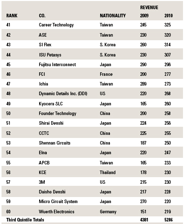
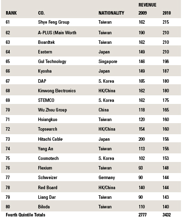
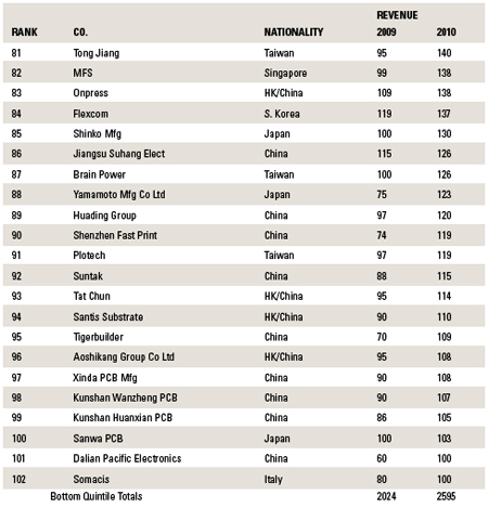
The annual rankings of the world’s largest PCB fabricators are, once again, dominated by Southeast Asia.
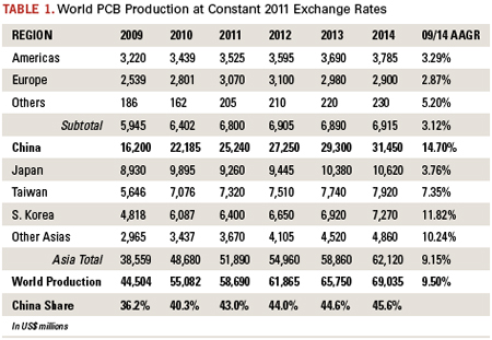
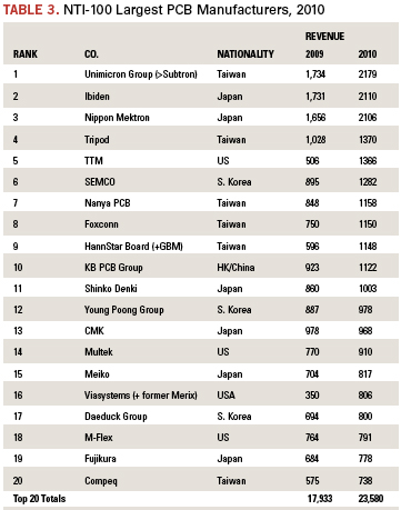
Worldwide printed circuit board output grew 23.8% year-over-year in 2010, fueled by – where else? – China, which grew 37%. Considering the ongoing and near-term expansion taking place in China, the nation’s PCB output will outpace all other regions per Table 1. The 102 largest (by revenue) fabricators produced approximately 80% of the total worldwide output in 2010. As we’ve noted many times, there is a clear trend that the bigger companies grow faster than the smaller ones.
In this annual report, we present a list of world’s top 102 PCB makers in 2010, and discuss their trends by analyzing the data from various angles.
Unlike previous years, we did not separate flexible printed circuit assembly (FPCA) from the totals because it is very difficult to separate the assembly values from the total output of those fabricators. Most large flex circuit fabricators generate a major portion of their revenues from assembly, however.
Also, some major mergers and acquisitions took place during 2010. Regardless of the dates of acquisition, these activities are assumed to have taken place on Jan. 1. Finally, the fiscal years of AT&S and most Japanese fabricators ended on March 31.
Exchange Rates
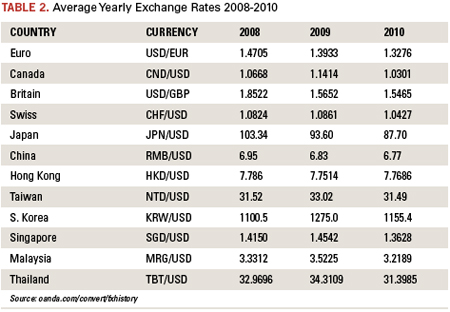
Exchange rates play a major role in the rankings. Taiwan manufacturers seem to convert their NT dollar-based output to US dollars every month. In this report, the author used “average exchange rates” to convert output in local currencies into US dollars for comparison purposes, as listed in Table 2.
The output reported by some Chinese makers included value-added taxes (VAT), which have been deducted. Moreover, close to 1,500 factories in China are operated by more than 1,100 manufacturers. As the author is not fluent in Chinese, he may have missed some important manufacturers that own multiple factories under different names. Every effort will be made to improve the data through better understanding of Chinese makers. Revenues of some manufacturers such as Foxconn (FAT) are based on calculated guesses, because the company does not break out its revenues. (If you know, please inform the author.)
Finally, keep in mind the rankings are “relative,” not “absolute.” If readers are dissatisfied by the rankings in the tables, please make your own corrections and judgment. Also, the author made maximum efforts to present as accurate a number as possible, but given human fallibility, there may be some errors. Please excuse the author for any errors, for which he takes full responsibility.
Summary of Top 102
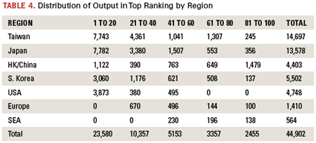
In 2010, a total of 102 companies had PCB sales of $100 million or more (Table 3). Total (domestic and overseas) production by Taiwanese PCB makers in 2010 is estimated to have been $17 billion, while No. 2 Japan topped $14 billion. These two countries accounted for 56% of the world production. Table 4 shows why. Their respective investments in China and Southeast Asia in fiscal 2011 will amount to approximately $2.5 billion, which puts these two countries in position to continue to dominate world production.
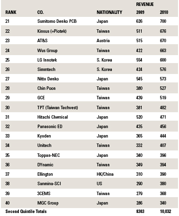
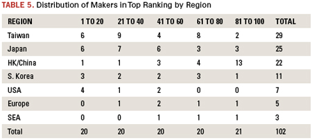
Hong Kong and Chinese fabricators are moving onto the list quickly, as one can see from Table 3 (an aggregate $1,379 million in the bottom quintile) and Table 5 (13 entries).
US-based fabricators actually build more boards offshore than they do in the US. To wit, it took about 320 US fabricators to produce $3 billion in 2010 domestically, while just six US-based fabricators (TTM, Viasystems, Multek, M-Flex, Sanmina-SCI and 3M) produced some $3.1 billion overseas. Because of their vigorous investment overseas, offshore production by US-based manufacturers will continue to grow, while domestic production will oscillate around the $3 billion level.
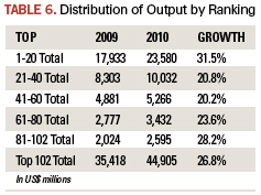
Table 6 underscores the “big get bigger” trend. At the same time, the growth rate of smaller manufacturers ($80 million to $150 million per annum revenue) is greater than their middle-class counterparts. This is driven by the China-based manufacturers, while mid-tier fabricators in “the west” are stagnant in terms of revenue growth. Big fabricators continue to expand because their big customers do not wish to increase the number of suppliers. Small ones have no fear. Middle-class makers are sandwiched between these two classes.
Dr. Hayao Nakahara is president of N.T. Information; This email address is being protected from spambots. You need JavaScript enabled to view it..
Ed.: Due to last-minute changes in the data, the original posting of this article indicated 101 fabricators had sales of $100 million or more in 2010. In fact, there were 102 such companies. PCD&F regrets the confusion.
Listen: Your SPI might be trying to tell you something.
Does anybody really believe that in 2011 three-fourths of all SMT defects are generated in the print process? Of course not. But we accept this spurious, decade-old, seemingly baseless statistic on stencil printing without question because we know how important a good printing process is to a profitable SMT assembly operation.
So we buy super-expensive inspection machines and reconfigure our assembly lines to accommodate them. We tout their superior GR&R of less than 10%. But when the inspection machine flags a print as bad, we have an operator look at it under the microscope and pass it down the line if it looks good to their “trained eye.”
Seriously? Then why purchase the machine? What’s the point of setting specific inspection parameters on a sophisticated tool, only to overrule them with far coarser and less accurate measurements? I’ve heard a number of reasons for passing flagged prints down the line, but to me they sound more like lame excuses than valid justifications.
When an inspection system fails a test specimen because a measurement does not meet user-defined criteria, I think it is up to the person who set the criteria to investigate why. I’ve spoken with a number of SPI power users, and they all echo similar thoughts on the topic: “When the machine fails prints, it’s trying to tell you that something’s wrong. You have to listen to it and do some engineering to find the root cause.” A few of the gurus shared interesting stories in support of their assertions:
During the validation testing of a brand new, electroformed stencil, the SPI system flagged half the prints for an odd combination of excessive and insufficient paste volumes. Typical defect modes on these PCBs might be one or the other, but rarely are the modes so mixed. The deposits and apertures looked fine under the microscope, so the engineer measured the stencil thickness in all four corners of the print area. That’s where he found the cause of the variation – a thickness differential of over 0.0025" (that’s 50% of the foil thickness itself!) presumably caused by current density fluctuations during the electroforming process.
A different assembler found a similar stencil problem when firing up a new product on his line. The print volumes on one QFP kept reading high, but the prints themselves looked great: nice bricks with straight sides and flat tops – no peaks, dog ears, strings, or other visual indicators of excessive paste. A series of measurements revealed that the stencil supplier had mistakenly cut a 0.006" foil instead the 0.005" that had been ordered. Had the engineer simply permitted the visual assessment to override the machine’s measurement without investigation, that stencil would have been placed into production, and would have likely caused lower yields due to suboptimal solder volumes; small features would have gotten less solder than they needed due to decreased area ratios, and larger features would have experienced more bridging due to the excessive volumes and slumping. The resulting yield hit would likely only be a couple percentage points. It could have flown under the radar for a long time, given that this was a new product and there was no baseline for comparison.
Another series of excessive volume readings – not necessarily rejects, but readings consistently in the 130% range – led engineers at a third assembler to measure the stencils and PCBs. They found the PCB pads were overetched by nearly 0.002", barely meeting the minimum size specification. But the pads met the spec, so the PCBs could not be rejected for quality reasons. The stencil apertures were already cropped for fine-pitch devices, so the size mismatch was about 0.001" – just enough to cause minor gasketing problems and permit excess paste to pump out along the gap. Understanding both the root cause and the degree of risk associated with running higher paste volumes, the engineers decided to open the upper tolerance limit for the remainder of the PCB lot. While I don’t normally advocate opening inspection tolerances to eliminate “false” calls (not truly false calls – just the ones that would be foolishly overridden anyway), in specific cases like this, it makes perfect sense. In fact, that’s why we like our tolerances to be programmable in the first place.
Three different PCB assemblers, three different stories on why we should listen to what our SPI systems are trying to tell us, and in all three cases, a little engineering legwork found the root cause of the problems. Interestingly, in all three cases, the printer and paste were working just fine.
Stencil printing is not just about the printer and the paste; if it were, the process would be a whole lot easier to manage. It’s about the entire system, including PCBs, stencils and squeegees (or print heads), and it’s the systemic interactions that make the process complicated, interesting and fun.
Next time the SPI flags bad prints, don’t pass them down the line with the assumption that the printer is fine. It probably is. While the SPI machine can’t tell you exactly what is wrong in the print system, it can tell you that something is wrong, and it’s up to you to listen to it, identify the root cause, and try to prevent the problem from happening again. After all, that is what process engineers get paid to do, isn’t it?
Chrys Shea is founder of Shea Engineering Services (sheaengineering.com); This email address is being protected from spambots. You need JavaScript enabled to view it.. She wrote this article on behalf of Christopher Associates (christopherweb.com).