Neck-downs and vias are common “choke points” for current, but there are design solutions.
PCBs get hot. This is especially true of modern PCBs, packed with power-hungry ICs dissipating more heat than ever. But heat generated by the ICs isn’t the only consequence of their thirst for amps. The power distribution network, or PDN, must be designed to provide adequate DC current-carrying capability; otherwise additional heat can be generated on the board itself.
It is difficult to design a PDN that meets the high current demands of today’s ICs. Not only has the amount of current increased, but so has the number of different voltages used by the ICs. This means that power planes have to be segmented into multiple different islands, and trying to piece together all those different islands can often lead to neck-downs in the plane shapes. Additionally, lower voltages are being used – some less than 1V – which means there is very little margin for any voltage to be lost due to resistance in the PDN. And, of course, there is pressure to lower PCB costs, which limits the number of plane layers used in a design.
Common problems associated with inadequately designed PDNs include voltage drop, excessive current in vias, and excessive current densities in some area of the board. Drops in voltage can result in insufficient voltage at the IC power pins, which can lead to IC malfunction. Excessive current densities can lead to board damage and disconnected power in extreme cases, but will also result in board heating. Heating of the board by the PDN contributes to the overall heating problem on the board, and can reduce IC life.
These types of issues can be pinpointed and eliminated during the design phase through the use of analysis tools. One of the types of power integrity simulations performed is a DC drop analysis, or IR drop analysis, so named because it simulates the drop in DC voltage caused by current (I) traveling through the resistance (R) of the planes. Power planes can be mapped out in the pre-layout stage, or completed PCB designs can be analyzed to pinpoint possible neck-down areas, such as the area shown in Figure 1.
Such areas of high current density need to be eliminated, and these areas aren’t confined to neck-downs in the planes. Vias are another common “choke point” for current. Knowing how many vias to use to transfer power from one layer to another, or to connect a voltage regulator module (VRM) to the rest of the circuit, is not always intuitive.
Thermal analysis. It is also not straightforward to extrapolate temperature rise from a given current density. Many variables affect how the heat will dissipate, and the resulting temperature rise for that location. For instance, the method of connection of the “hot spot” to the rest of the plane is a large factor. Copper conducts temperature, not just electricity. Also, the percentage of metal in the surrounding layers above and below this area, as well as the board environment, will affect the temperature. These are the types of factors included in a thermal analysis. By performing a thermal/IR drop co-simulation, these hot spots in the planes can be examined for precisely how hot they will get.
Thermal simulations model all three methods of heat transfer: conduction, radiation and convection. Heat is conducted from the ICs through their pins and then throughout the board. Heat is radiated from the ICs and from the board. Heat is also transferred through convection – naturally, opposite the direction of gravity, as well as through forced convection if there is some type of fan or blower in the system. When a high current density area exists in a PDN, it acts like another heat source, and that heat gets dissipated by a combination of these three methods of heat transfer.
Voltage drop and temperature are actually closely related, because the resistance of copper changes with temperature. In fact, copper conductivity changes 4% for every 10˚C of temperature change. A temperature range of 80˚ equates to a 32% change in copper conductivity, which is quite significant. As such, to determine the actual current densities in the copper on the board, the temperature of the board must be known. And in order to determine the temperature on the board, the current densities on the board must be known. Hence, there is a need for a co-simulation between IR drop and thermal analysis in order to generate accurate results.
So, to accurately predict the temperature rise caused by areas of high current density, the temperature of the board must first be known. This requires, at the very least, modeling the power dissipation of the components, their connection to the board, the board itself, and the environment the board is in. With this information, thermal simulation can be used to develop a thermal profile of the board, which can then be fed into an IR drop simulation to ensure the appropriate copper conductivity. The results of the IR drop simulation can then be fed back into the thermal simulation to include the effects of power being dissipated by the PDN, and this back-and-forth iteration of simulations can continue until the simulators converge on a solution. An example of such a simulation is shown in Figure 2.
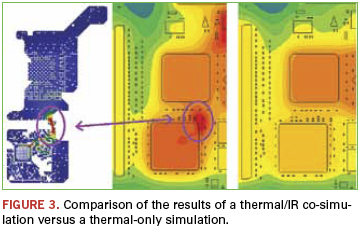
This simulation includes the heating effects of a 1.5V plane that is feeding two larger ICs on the right side of the board. Thermal effects are a little different from electrical effects in that it is much more difficult to isolate them. Electrical effects can be examined on a per-net basis. For example, a single signal net can be examined for signal integrity, or a single power net can be examined for power integrity. In thermal analysis, the entire board, including its environment, needs to be analyzed at once. As such, for maximum accuracy, all the power nets on the board, including the ground net(s), should be analyzed at once, since they all interact. In this example, more clearly depicted in Figure 3, there is obviously an area of increased temperature on the board corresponding to the area of high current density on the plane. Comparison against a thermal-only simulation reveals the importance of including the heating effects of the PDN.
More important, the heating effect of that plane shape neck-down is accurately characterized, and provides valuable information in driving a design change on the board. In this instance, the easiest solution would be to eliminate that neck-down on the plane shape. However, if that plane is feeding multiple voltages throughout the board, that may be difficult. Another solution may be to add another shape on another layer to help “bridge” the gap where the neck-down occurs, and stitch it to the existing plane shape using vias. Such a fix could be analyzed by performing another simulation.
Other hotspots. It is important to note that such plane shape neck-downs aren’t the only PDN design issues that can cause thermal problems. On any design with BGAs, especially finer-pitch BGAs, such problems will naturally occur in the breakout area beneath the BGA. There, the power planes are often perforated with antipads from signal and ground vias, forming a narrow web of copper to feed current to the power pins. These areas are commonly areas of very high current density, which can cause the same type of heating issues (Figure 4).
These areas can be especially problematic because they are already the highest temperature areas on the board, because they reside beneath the ICs. The ICs are typically the most significant sources of heat on the board, and the areas beneath them tend to be the hottest areas on the board as a result. Adding additional sources of heat to these areas – areas of high current densities caused by perforated planes – leads to higher temperatures on the IC and ultimately reduced component lifespan. For every 10˚ above 100, the mean time between failure (MTBF) of a component is reduced by as much as 50%.
Power pins and stitching vias can be another area of the design at risk for thermal issues. It is important that any VRM attached to the power planes be attached with adequate power pins and/or stitching vias, so that the current is distributed and temperatures of those pins and vias are kept relatively low. The same is true for vias stitching multiple power planes together.
Thermal issues are often solved in a variety of ways: adding heatsinks to components, changing airflow, or separating hotter components, to name a few. Thermal issues caused by inadequate PDN design have one simple solution: add more metal. This may mean widening traces carrying significant current, eliminating neck-downs from plane shapes, using thicker copper on the planes, or adding more stitching vias where necessary. The solution is simple. Through analysis of the power distribution system prior to building the boards, such problems can be quickly identified and resolved. This will result in designs that are more reliable and last a long time.
Patrick Carrier is product manager, high-speed PCB analysis tools, Mentor Graphics (mentor.com); This email address is being protected from spambots. You need JavaScript enabled to view it..
The month of May is quickly winding down, and the June trade show season is fast approaching. On June 13, the JPCA Show will open its doors at Tokyo Big Sight. The three-day event is the largest trade exhibition for the printed circuit industry. Most agree that the JPCA Show is always a great source of information for both technical and business tidbits. However, in my opinion, it is a great source of information to predict the future for the Japanese printed circuit industry.
Let’s first look at some data for the last eight years. Listed below are the annual revenue numbers for the Japanese PCB industry (provided by METI), as well as the percent change from the year below:
Growth rates were positive year over year from 2004 – 2007. There was a big hit to revenue during 2008 and 2009 at the peak of the global recession. Markets in every country suffered during this period of time. The printed circuit industry did recover nicely during 2010 and posted a 15% increase over 2009. The entire industry did not get caught up in the recovery wave, so analysts predicted slow and steady growth for 2011. Unfortunately, this did not come to fruition. Not only did revenue fall by 15% compared to the previous year, the industry also posted its lowest annual revenue in eight years. The bad news for the Japanese industry is this double digit negative growth did not happen in Taiwan, the U.S. and Germany. Taiwan has set new revenue records for this same period of time, and the U.S. and Germany are showing small but positive increases.
Most business analysts from the Japanese printed circuit industry recall the business environment in the U.S. after the IT bubble crash in 2001. The U.S. PCB industry suffered significant declines, and most of the larger sized circuit manufacturers quickly disappeared from the industry. The IPC Apex Expo is a large trade show for industry and attracts worldwide audiences. Participation dropped dramatically in 2002, and the show never recovered.
I think the JPCA Show 2012 will be very positive and upbeat. I do not think I will see any signs pointing to an industry melt down. However, I will be able to network and gather market information by communicating with the industry experts and management teams during the show. Some of this chatter that I can pick up during the show is a more realistic outlook for the industry in the upcoming year. I look forward to sharing some of these opinions in one of the upcoming newsletter.
Dominique K. Numakura DKN Research, www.dknresearch.com
Headlines of the week (Please contact This email address is being protected from spambots. You need JavaScript enabled to view it. for further information of the news.)
1. Asahi Kasei (Major chemical company in Japan) 5/14 Has started the construction of the new manufacturing plant in China for the photo dry films of PCB with an annual capacity of 120 million square meters.
2. Mirie Automation (Equipment manufacturer in Taiwan) 5/15 Has been getting a lot of new orders manufacturing equipment from Chinese LCD manufacturers for 5G, 6G and 8G lines.
3. Bridgestone (Major tier suppler in Japan) 5/15 Has decided to close the e-paper business because of extreme price competition in the market. The manufacturing will be terminated by October.
4. Panasonic (Major electronics company in Japan) 5/15 Has rolled out a new 65” size white board with PDP technology for business use. 85” and 103” size products will be commercialized by the yearend.
5. Nippon Electric Glass (Major glass material supplier in Japan) 5/16 Will open a new manufacturing and marketing subsidiary in Korea for the local customers of LCD glass substrates.
6. Furukawa Electric (Major cable manufacturing company in Japan) 5/17 Will ship out the first high voltage (275 kV) super conductor cable from Ichihara Plant. Its field test will be conducted in China.
7. Ricoh (Major electronics company in Japan) 5/21 Has developed a new lead free piezo material applying inkjet printing process of PZT for actuator devices.
8. Kobelco (Major steel supplier in Japan) 5/23 Has developed a new fuel cell separator material by coating carbon material on titanium. It reduces the contact resistance to half compared to the other metals.
9. Sharp (Major electronics company in Japan) 5/24 Had agreed to have a procurement alliance with Toppan Printing and Dai Nippon Printing for the color filter materials of LCD panels in Sakai Plant.
10. New Japan Radio (Device manufacturer in Japan) 5/24 Has established the first volume production process of the copper wire bonding on aluminum pads for power semiconductor chips.
DKN Research Newsletter May 27, 2012 (English Edition) Electronic Packaging Industry News from Japan & Asia (www.dknresearchllc.com)
Most product cost is determined in design, before it ever reaches production.
OEMs constantly seek ways to cut product cost and time-to-market. The advantages of a shorter time-to-market and lower costs of an end-product are evident: market attraction improves, lifecycle extends, development cost reduces, etc. This is far from a trivial mission, and different managers look for different ways to achieve these objectives. One strategic path leading to attaining these objectives is DfX methodology. DfX (Design for Excellence) is an efficient tool with a proven record of accomplishment with which we can ensure proper execution of electronics products the first time.
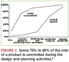
Research indicates that OEMs that develop electronics products and have implemented DfX methods stayed within 82% of their development budget, performed 66% less repair rounds and saved $26,000 in those rounds they did perform.1 Other scientific work2 indicates that approximately 75% to 85% of the cost of an electronic product is determined in the design phase, while the actual product costs increase significantly, of all places, during production (Figure 1).
As the design process advances, the window of opportunity to introduce changes becomes smaller, and the cost of introducing change grows, in some cases exponentially. For example, introducing a change after putting together a prototype will entail a new PCB layout round, execution of an engineering change order (ECO), ordering a replacement version, reproduction, inspection of quality and reliability, renewed meeting of standards, delay in supply to customers, etc. In other words, taking into consideration problems that may arise during production and assembly during the design phase proves to be an efficacious method for reducing costs and increasing yield.
It is true that implemention of DfX requires further investment of time by the organization during design, yet research indicates that as a result of this extension of time, the product’s overall time-to-market drops by approximately 40%.3
This requires an understanding that quality control, by itself, does not suffice for the task of prevention of problems. The fundamental of success of an electronics product is a sound design, maintaining an open and productive channel of communication between the designers and production, based on accumulated knowledge and experience. As part of DfX, we remain aware that failure may occur in the future, and implement working methods to prevent it from happening.
Failures in design of the electronics product can take place due to incomplete exchange of information between the electrical, mechanical and PCB layout design; failure to understand the shortcomings and capabilities of production; and unrealistic customer expectations regarding the process of development of a new product in matters of reliability and time-to-market. DfX’s purpose is to ensure consistent and continuous production throughout the supply chain, with a minimal number of failures.
The DfX methodology consists of several sub-topics, according to the various stages in the product lifecycle. Every topic relates to a different stage in the production cycle and is accompanied by instructions pertaining to the actions to be taken in the design stage to prevent failures. These topics include DfM (design for manufacturing), DfT (design for testability), DfR (design for reliability) and DfE (design for environment).
To demonstrate this, following are several key rules how to properly implement DfX.
Learn from the past. Albert Einstein said, “The only source of knowledge is experience.” When developing new products, consult the past. Failure to meet quality, customer complaints, reasons for product recall, and so on are all sources of information to draw from. To this end, we are required to document such incidents in an orderly way, analyze them and implement procedures that will prevent their recurrence. A cross-organizational brainstorming of every element taking part in the project may well be a way to achieve this.
Stick to norms as much as possible. Adhere to standards as much as possible at all stages of product development. This is true when engaged in design, layout, choice of components, procurement, production processes, etc. Developing product using existing standards helps cut time-to-market, simplifies processes and minimizes risk of errors. Take, for example, a non-standard component. If we choose a component failing to meet the norm, we expose ourselves to a higher price tag, because the part is less common among all the suppliers, thus less governed by laws of competition and (likely) produced in smaller batches. Second, as a result of the need to replace the item, the time to deliver may stretch, and consequently, we may presume that the supply chain will be disrupted. It may be difficult to find a substitute component. Avoid reinventing the wheel; stick to norms as much as possible.
Reduce the number of components in a product. One of the best ways to reduce production costs and enhance product quality and reliability is to reduce the number of components. When using fewer components, the cost of acquisition may be reduced by placing a large order of one item, rather than a small order of several items. In addition, as the number of components in an electronic circuit determines the assembly cost, reducing the number used will lower that cost, respectively. Further, reducing the number of components will result with less risk of faulty items and quality issues during assembly. Consider these examples: First, designated component library, including an AVL (approved vendor list), ensures that a new product would use known components. Second, components that can be used in several applications may cause an increase in direct costs, but in general, the overall cost of all the components will decrease. Third, ordering whole assemblies from a subcontractor avoids dealing with putting together these subassemblies.
Design for Lean production. The main principle of designing for Lean production is that whatever does not add to the product’s value is garbage to be discarded. As part of this design, cut down on production processes as much as possible through use of automatic assembly over manual (e.g., SMT components instead of manual insertion through-hole parts). The manual assembly to be performed should be simplified to such degree as to avoid questions and errors, as well as to help turn assembly automatic at a later stage. Refrain from additional production processes, where possible; e.g., design boards with components on one side instead of both sides by reducing the area of components or increasing the area of the printed circuit board. Design for Lean can help save a great deal of time in production and improve product quality.
When it comes to production, stay away from technological extremes. Make a distinction between the product’s development and its production. When we develop the product, we may be interested in taking the technology to an extreme to differentiate our product from competing products in the marketplace, as well as to offer our customer added value. In its production, we should take the opposite approach. Since production is not added value for us, we should simplify it and base it on existing technologies, ensuring higher quality and reliability. So, for example, choosing a component with a 0.4mm pitch would be preferred over a 0.3mm pitch component; a 0402 package would be a better choice than a 0201 package, and choosing a 10 mil trace width would be better than choosing an 8 mil.
Develop work methods to nullify failure. As we know, Murphy’s Law never rests. If anything can go wrong, it will. Anticipate failures and work to prevent them from happening in the first place. For instance, a clear and comprehensible product assemble file should be prepared for every worker of the production line. To avoid confusion and interference, the instructions should be specified in a methodic and unequivocal way. To prevent duplication, instructions should be listed only in one place in the file. Reduce text use as much as possible; use images and visualization in its place. In this context, it would be advisable to plan the product’s assembly process so it will be assembled in no way but the proper one. Improper assembly should be prevented by employment of asymmetric holes, stops, etc.
Integrate and coordinate design and layout elements and production and assembly elements. Whenever a PCB is designed, its production should be taken into account from the start. The planning and layout teams should be synchronized at the best possible level with the production and assembly teams. To reach a complete optimization of the circuit and electronics product throughout production, initiate thinking processes, combining the planning and PCB layout with production and assembly elements. Ensure that every critical objective of the process is known, considered, controlled and eventually, achieved. These objectives include product cost, desired level of quality, reliability, regulation, time-to-market and customer satisfaction.
The great victors of today’s competitive technological world are those companies that can deliver to their customer an innovative product that holds an added value over their competitors. Development of an innovative product is an imperative but insufficient condition to attain these objectives. Organizations wishing to achieve these goals should reduce their production costs and shorten the product’s time-to-market. Implementation of DfX will improve company performance by ensuring the right job is performed correctly from the beginning.
References
1. Aberdeen Group, “Printed Circuit Board Design Integrity, The Key to Successful PCB Development,” 2007. 2. Martin Tarr, “The DfX Concept,” University of Bolton, 2007. 3. D. E. Carter, and B. S. Baker, Concurrent Engineering: The Product Development Environment for the 1990s, Addison-Wesley Publishing, 1992.
Arbel Nissan is COO at Nistec (nistec.com); This email address is being protected from spambots. You need JavaScript enabled to view it..
In 2012, PCB designers say their salaries are rising and their challenges are staying the same.
If PCD&F learned anything from this year’s designers’ salary survey, it’s that the overall picture looks remarkably similar to that of 2011.
In late February through March, PCD&F compiled data from 467 bare board designers. The survey, which was conducted online, covered salaries, job functions, titles, types of projects, benefits, education, experience, career concerns, and location, to name some. Results are intended to paint a portrait of the status of design industry jobs, as opposed to a thorough scientific account.
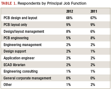
Sixty-eight percent of the 467 respondents listed their principal job function as PCB design and layout – the most common response by far (Table 1). Next was “PCB layout only,” which garnered 9% of responses, flat with 2011, followed by design/layout management (8%, up two points from 2011), and PCB engineering (5%, down from 8% last year).
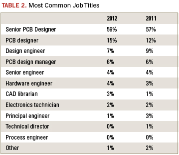
Of those surveyed, 56% are senior PCB designers, down just one percentage point since the 2011 survey (Table 2). The second most selected job title was PCB designer, with 15% of responses, compared to 12% in 2011. Design engineers make up 7% of this year’s respondents, down from 9% in the last survey. Other job titles in 2012 include PCB design manager (6%), senior engineer (4%), hardware engineer (4%), CAD librarian (3%), electronics technician (2%), principal engineer (1%), and “other” (1%).
Designers are still predominantly a veteran crowd, with 53% (compared to 54% in 2011) indicating more than 20 years’ experience in the industry. Twenty-one percent of respondents say they have more than 30 years under their belts, up from 18% in 2011. Sixteen percent indicate 11 to 15 years, 21 to 25 years, and 26 to 30 years, respectively, while 13% say they’ve been in the business for 16 to 20 years. Seventeen percent surveyed are relative newcomers, with 10 years or fewer of experience (3% more than in 2011); only 7% of those respondents indicate five or fewer years.
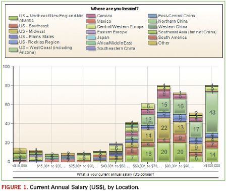
In response to reader requests, PCD&F sought more detail on where respondents are located with this year’s survey. As with last year, most who took the survey are located in the US (73%); this figure is down three percentage points from 2011 (Figure 1). This year, PCD&F also broke the US into regions. Twenty-three percent of respondents are located on the West Coast (including Arizona). Eighteen percent are in the Northeast/New England/Mid Atlantic section of the US, while 15% live in the Midwest. Eight percent are in the Southeast part of the US; 5% are in the Rockies region, and 4% live in the plains states.
Nine percent of respondents live in Central/Western Europe; 6% are in Canada; 3% are in Southeast Asia (not China), and 3% checked “other.” Only 2% of respondents reside in Mexico and Africa/Middle East, respectively. One percent live in Eastern Europe. Other areas of the globe are not statistically represented in the responses.
The bare board design field continues to be dominated by men; 86% of respondents are male, compared to 88% last year. And the industry is still aging. Fifty-five percent of respondents fall between ages 46 and 60, and another 10% are between 60 and 70-years-old. Ten percent are 41 to 45; 9% are 36 to 40; 7% are 31 to 35, and another 7% are 26 to 30. Only 1% of respondents are under 25. The same question continues to loom: With more designers reaching retirement age than those who are poised to replace them, what will the implications be in the next decade or so in terms of qualified workers? Educators, take note.
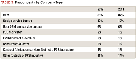
Designers still mostly work for OEMs (66% this year compared to 67% last year). Ten percent say they work for design service bureaus, flat with 2011 (Table 3). Six percent work for both, also the same as last year. Two percent work for EMS firms, compared to only 1% last year. Another 2% work for PCB fabricators, and 2% more work as consultants.
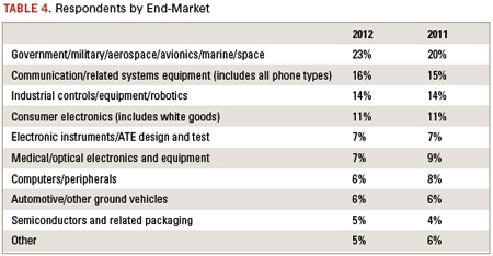
All end-markets are represented by the respondents, and the population by sector generally reflects the overall electronics end-market breakdown by revenue. The largest percentage of respondents, 23%, design high-reliability products (Table 4). Meanwhile, consumer electronics (including white goods) makes up 11%. Large companies continue to dominate. As in 2011, 40% of survey respondents work for companies that have more than 1,000 employees. Eighteen percent work at firms with 251 to 1,000 staff members, compared to 19% last year. Merely 14% work for companies with 25 or fewer employees, down two percentage points from 2011. Thirteen percent are among a staff of 101 to 250.
Surprisingly, a full quarter of respondents are unsure of their company’s approximate annual sales. Eighteen percent say they work for a firm with $5 billion or more in sales, up three percentage points from last year. The third highest response was $5 million to $49 million, with 15%. Nine percent work for a firm with $1 billion to $4.9 billion in sales; another 9% work for a firm with $100 million to $499 million in sales; 8% said $50 million to $99.9 million, and 7% indicated $500 million to $999 million. Only 9% work for a firm with sales less than $5 million, down from 13% in 2011.
Pay Hikes
The survey asked respondents to characterize current annual salaries in US dollars in five- to ten-thousand-dollar increments. Seventy-three percent say their salary exceeds $60,000, the same percentage as in 2011. Some 28% say their salary tops $90,000, down two percentage points from last year, with 17% of those respondents making six figures – up from 12% last year. Twelve percent make $30,000 or less, with 8% in the $20,000 or below range.
In the past 12 months, 69% of respondents saw their pay increase, compared to 70% at this time in 2011. Of that 69%, the bulk received raises of 1 to 6% (Figure 1). Five percent say their salary increased 7 to 10%, and some 6% saw pay raises of more than 10%. Seven percent indicated a salary drop in the past 12 months, up from 4% last year. The remainder say their salary hasn’t changed.
More than half (56%) of respondents didn’t see a bonus in the last 12 months, compared to 53% last year. Of those who did receive a bonus in the past year, 43% say it was 1 to 3% of their salary, up one percentage point from 2011; 29% say it was 4 to 6% of their salary (same as last year), and 28% received a bonus of more than 7% of their salary, down two points from the 2011 survey.
Health insurance topped the company benefits once again with 87%, up two percentage points from last year’s survey. Dental insurance coverage is provided to 75% of respondents, compared to 73% last year. Life insurance received 73% of responses, compared to 70% in 2011. Sixty-six percent say they have the option of a 401(k) or other savings plan, down two percentage points from the previous survey. Other benefits include an onsite cafeteria (50%); a stock purchasing plan (36%); an exercise facility (33%); a company pension or retirement plan (28%); telecommuting (24%); profit sharing (23%); relocation expenses (16%); sabbatical (6%); daycare (4%), and 7% of respondents say they do not receive any of these benefits with their firm, compared to 9% last year.
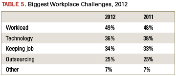
When asked about the biggest challenges designers expect to face in 2012, “workload” is still the top response with 49% of responses (Table 5). Technology is second, at 36%. A close third is keeping one’s job, with 34% of respondents concerned about their job security. Twenty-five percent say outsourcing is their biggest concern, and 7% say “other.”
The survey again asked designers what types of technologies they directly engineer, design or layout. As in 2011, the most responses went to 4 to 6 layer PCBs (84%) and double-sided PCBs (81%). Seven to 10 layer boards garnered 61% of responses; 58% say BGAs; more than half also work with 12 plus layer PCBs (53%); 47% of people say single-sided PCBs, compared to 51% last year. Other responses:
The number of new designs produced each year could be increasing based on the numbers. Six to 10 designs is still the highest response, with 29%, up from 27% in 2011. Eleven to 15 came in second with 18%; 14% say 16 to 20; 8% say 21 to 30, and 16% produce more than 30 designs each year. This figure is 5% higher than last year. Only 15% say 1 to 5 designs, which is 3% fewer than 2011.
The picture of education looks very similar to the responses in 2011. Again, only 5% say their highest level of education is a high school diploma. Sixty percent have “some college” or an associate’s degree, down from 62% last year. Twenty-one percent have a bachelor’s degree in engineering, flat with 2011. Only 5% have a bachelor’s degree in a non-engineering field, down one percentage point from the previous survey. This year, 9% say they have a master’s degree, which is 3% more than last year. Two respondents say they have a Ph.D.
The majority of companies encourage continuing education, with 55% of respondents saying their firm provides tuition reimbursement, down two points from last year. Fifty-three percent receive on-the-job training, and 45% indicate they have the option of attending classes at conferences, both flat with last year’s survey. Forty-one percent have company-sponsored classes; 28% have mentoring; college classes are supported by 21% of companies, while 20% of them do not provide any of these educational opportunities.
Slightly more respondents in this year’s survey have management responsibilities, but the majority are still not responsible for managing others. Seventy-six percent do not have other staff members reporting to them, compared to 79% last year. Nineteen percent say 1 to 5 people report to them, up 3% over 2011. Four percent say 6 to 10 people report to them, and only 1% are responsible for 11 to 20 other employees. One person who responded to the survey manages more than 20 people.
Thirty-three percent of respondents are IPC certified designers, compared to 36% on the last survey. Seven percent say they were laid off in the past 12 months, compared to 6% in 2011. A whopping 91% say they have the same job as they did at this time in 2011.
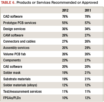
Of those who can recommend or approve product purchases, most get to weigh in on software tools. (Table 6). Twenty percent evaluate products, and 17% specify products. Eight percent can approve product purchases, and 19% lack authority to perform any of these functions, compared to 16% in 2011. Designers’ jobs and salaries look stable for 2012; the positive improvements that began in 2011 have maintained steadiness.
3D structures on high-speed signal paths can significantly influence transmitted signals.
Those involved in board analysis during the past 10 years will have noticed changes in signal speed and design applications. The dominant high-speed applications are high-speed memory designs and gigabit-per-second channel designs. At the end of the last century, engineers started routing differential signal nets on PCBs that could transfer data at rates exceeding 1 Gbps. The signals at such speed were initially used to build boards and backplanes in large communication systems. Demand for increasingly fast computation and information transmission continues to increase, with a substantial number of designs operating at multiple Gbps range. Advanced memory designs are moving data at 10 Gbps, and the latest SerDes communication standard is reaching toward 30 Gbps.
With signal speed changes come new challenges of solving design issues never seen before. The components of signal paths on boards and interconnects present problems, such as significant dielectric loss or impedance discontinuity from non-trace portion, which used to be ignored at lower signal speed.
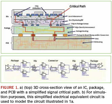
Figure 1a illustrates the three-dimensional cross-section of an IC with a SerDes channel, showing the die, its associated package and pins (or balls), the PCB, and the mechanical mounting of the package on the PCB; Figure 1b shows the electrical equivalent circuit. In this example, the impedance discontinuity contribution comes from the vias for signal switching layers, connectors enabling multi-board connections, and packages. To PCB designers, only via configurations are under their control in these discontinuity contributors.
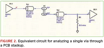
Via modeling. To understand modeling of the vias used in simulation, we’ll begin with a single via in a PCB stackup. Figure 2 is a schematic representation of the equivalent circuit. With slower speeds (that is, slower rise and fall times) common up to a few years ago, via effects were not significant enough to be concerned. Now, with signals having rise/fall times around 100 ps, via effects are noticeable and can cause signal degradation. The typical SI effects of the impedance discontinuity caused by true 3D vias can be seen in the plots in Figure 3.
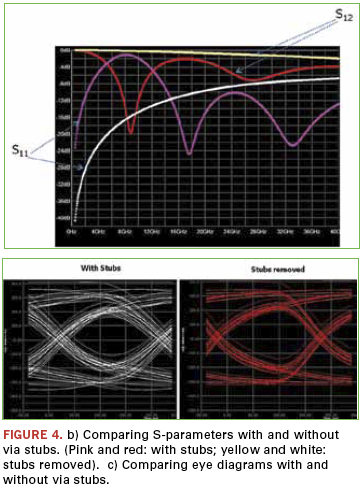
When simulating a complete channel, signal paths are analyzed using differential vias. Differential vias improve signal integrity, but can also cause signal degradation if the via stubs are not correctly configured. Via stubs not only cause SI issues, they can completely attenuate signals at certain frequencies.
Figure 4 shows analysis on a design with a pair of differential vias on a 16-layer board. The S-parameter plot (Figure 4a) and the eye diagram (Figure 4b) illustrate how via stubs can produce unwanted resonance peaks (8 GHz in the example).
The S-parameter plot shows that the via stubs (red and pink) produce several resonance points, at which point the signal component cannot be transmitted. With the stubs removed (yellow and white), there are no resonance points introduced. Similarly, the eye diagram becomes much smaller with the stubs.
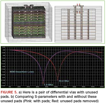
Effects of unused pads. The differential signal paths often enter on one layer and exit on another layer, transmitted between layers through vias. The unused via pads also can cause SI problems. Figure 5 shows the configuration of a pair of vias going through a board stackup of 26 layers. Leaving all these pads in place can cause a resonance peak at lower frequency. By removing the pads, the resonances are pushed upward in frequency, benefiting SI. Backdrilling is the best way to handle these problems, but removing the pads can help the problem when backdrilling is not possible.
Understanding the impacts from 3D structures on signal interconnects is important for designers to ensure good design practice. However, the most common case is to know not only whether there is a design problem, but also how much the effect could be and if a design can still work without significant modification.
To answer these questions, 3D modeling functions are needed to produce detailed results for studying structure behavior and making tradeoffs.
Effectively using 3D modeling. When effectively putting the modeling into practice on an actual circuit, the designer has a number of questions for which he is seeking an answer. Is there an SI problem? If so, what is the magnitude and source of the problem? Can the problem be solved without significant modification, and if not, how much modification is required?
Analysis tools must be capable of answering these questions quickly and accurately. Until recently, 3D analysis of a particular structure has been performed in a separate modeling environment from the general PCB (or package) layout and SI simulation tools. This is adequate for simple structures that can be manually created. But for complex or arbitrary geometries, a standalone tool requires database translation first to get structure geometries imported from layout or port-route analysis environment, which commonly is owned by third parties. In addition, the translation itself can introduce errors during conversion. Conversion can be time-consuming and risky. Also, most tools to date have required that the user have strong electromagnetic experience to use them effectively.
Initial analysis should begin in the pre-layout planning stages. As you could see in the analysis of via stubs, understanding the effects of vias before actually beginning the layout can permit potential problems to be discovered and mitigated before anything has to be unraveled. For this early analysis, it is possible to use a separate 3D tool without much difficulty.
Once pre-layout studies have been completed, the structure is put on board with other nets routed, components placed, and holes drilled. Even so, the resulting PCB layout can still have coupling with some components, and the previously understood behavior can be affected; there may also be new noise sources on the board after layout as well. When this happens, the discontinuity effect from the particular 3D object must be simulated again, including its immediate neighbors, such as nets, other vias, etc. At this stage of development, using a separate 3D tool to analyze the more complicated geometry is very, very tedious.
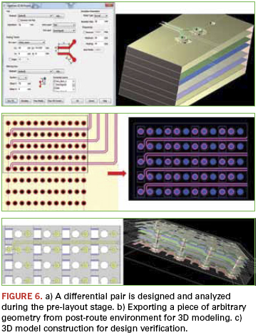
Better is to have a 3D modeling engine integrated with a general layout and SI environment. The integration then permits detailed structure design/tuning in the pre-layout stage and discontinuity effect verification at port-route level. This solution is illustrated in Figure 6. In this example, Mentor Graphics’ HyperLynx was used first to specify a pair of differential vias in the pre-layout environment (Figure 6a) and determine if a single stitching (or ground) via is sufficient for the required switching rate.
After layout, the designer can select the interested area in the routed design where other nets and structures have been placed near the vias of interest, and tell the tool to export the piece of arbitrary geometry to the 3D modeling engine for creation of proper 3D model (Figure 6b). The resulting model (Figure 6c) highlights the coupling effect to the pre-defined differential via structure. Because the position of geometry cut on the board is known, the 3D model can be connected back to the interested nets in channel simulation. Armed with these data, the designer can then decide if the channel budget can tolerate the effect, or if more design work is necessary to reduce the extra noise.
Dr. Zhen Mu is a product market manager at Mentor Graphics (mentor.com), responsible for signal integrity and power integrity products for printed circuit board and package analysis.