There is a popular social network game that many of us may not know exists. Annual revenues from this market have grown from a few million dollars to over $3 billion in just five years. It is a now a main topic of discussion in Japanese business circles because of its phenomenal growth rate.
It was 50 years ago today when a then 33-year-old scientist at General Electric invented the first practical visible-spectrum light-emitting diode, a device that GE colleagues at the time called “the magic one” because its light, unlike infrared lasers, was visible to the human eye.
Dr. Nick Holonyak, Jr. could not have known then the door he was opening, but today LEDs are not only the foundation of a massive government-driven push to eliminate the popular (but higher energy consuming) incandescent, but also a potentially enormous market for the manufacturers of LED and driver printed circuit boards at the core of LEDs.
LEDs contain metal or graphite core bare boards, generally with lead-free solder paste. They are not easy to rework, on account of their heat-sinking core. The LED components are typically surface-mounted, although some versions have radial-leaded parts, explains Scott Maudlin of LEDnovation, an OEM of residential and industrial LED lighting.
Many PCB and EMS companies have an opportunity to play in this market today, thanks to one man's bright idea 50 years ago. We owe Holonyak a big round of applause.
Done right, routing by hand offers several advantages over autorouters.
Many engineers wish for some kind of “magic wand” autorouter to do their job. That’s not going to happen, at least in the near future. Therefore, we have to rely on manual routing. Despite its importance and effectiveness, designers still have difficulties routing boards manually. Here we’d like to share some experience about effective manual routing. All mentioned are applicable to most PCB CAD systems.
In our experience, a manually routed board is more likely than an autorouted board to become a working prototype. But if a printed circuit board designer lacks experience and understanding of the circuit, manual routing can become their worst nightmare.
Manual routing allows the engineer to apply all their experience to the design. An autorouter is an algorithm, and as such is limited in performing analysis or making decisions.
Tip 1. Big at the center. The key to quality prototype is a rational placement of components on the board. Leave sufficient space between the packages, considering the possibility of rerouting and additional traces. Complex ICs should be located at the center of the board, not near the edge (Figure 1). Before routing, move components around the board, trying to decrease the length of connections and total number of intersections. Use 3D preview (if supported) to visualize the prototype and check component layout.
Tip 2. Behind the grid. Grid size should be aliquot (exactly divisible) to the pitch of component (usually two times smaller). Use the same grid size for routing nets and placing components. Turn it OFF for narrow passes.
Tip 3. Layers. The manual routing strategy usually depends on the number of layers of the board. Single layer boards are just about the price. Traces usually have a lot of curves. These boards are good for very simple projects. Jumper wires are very common.
Double-sided boards are the most popular for hobbyists. Usually these boards have plenty of ground net copper pour islands, connected into one net by lots of vias (Figure 2). Multilayer boards are used for complex projects (fanouts, innerlayers, etc).
Tip 4. Listen to manufacturer. Always leave free space while routing, and make traces a bit wider than manufacturer minimums. Apply all your skills in order to make the board better.
Tip 5. Fewer vias. Create as many via-free connections as possible. Vias should be avoided, because they are costly, take a lot of space on the board, and lead to signal integrity problems in high-speed buses. Therefore, if unavoidable, place vias closer to component pads (Figure 3). This should mask wave impedance irregularities. Try to follow this rule: one via for any trace between a surface mount and through-hole pad, and two vias for the trace between two surface mount pads on average.
Tip 6. Up and down. Try to follow opposite routing directions on different layers. For example, vertical traces on the top layer and horizontal on the bottom. This layout is perfect for double-layer boards (Figure 4).
Tip 7. Power pours. Power and Ground traces should be wide enough to withstand high-amperage current with low impedance. If the trace is going from one layer to another, several vias should be positioned parallel. Copper pours are much more reliable than traces (Figure 5). Make sure that pours don’t have narrow regions.
Manual routing is limited only to the skills of designer or engineer. It’s a great oportunity to express yourself, to be not just the engineer, but an artist. The main disadvantage is that manual routing is time-consuming, and thus not applicable in some cases. Some designers prefer manual routing, others automatic, and some use a combination of each.
Alex Mykhaylenko is an electronic engineer and Vlad Khomenko is a technical writer for Novarm Ltd. (novarm.com); This email address is being protected from spambots. You need JavaScript enabled to view it..
A new Web-based training program teaches cost-savings using best-of-breed design and purchasing practices.
Web-based instruction is a growing market, and developed correctly, offers many advantages over traditional classroom settings. A new comprehensive online workshop aimed at electronics designers and engineers is the first to focus specifically on industry-specific environmental considerations and compliance.
The rationale is clear: Some 80% of the environmental impact of a product occurs during design phase, says Technology Forecasters Inc. (techforecasters.com), which developed the tool.
The training program, DFE Online (techforecasters.com/dfe-online), is really a self-paced electronic workshop. Made up of eight modules, it combines voiceover narration with clear pictorials, drawings, text slides and even links to short, hosted videos to explain a variety of concepts related to designing electronics products for the least environmental impact.
“Designers and the product launch team need to understand the basics of efficient environmental design, so when they do it, they do it in the most efficient, cost-effective way,” explains Pamela J. Gordon, founder and president of TFI.
The developers did a good job considering how an engineer might best grasp and absorb information. Data and images are delivered in multiple formats. There’s even an optional quiz after each of the modules, to help ensure the participant understands the subject matter. If they answer 10 of the 12 questions correctly, a certificate is issued.
Topics range from hands-on engineering advice to the business cases for Design for Environment (DfE). They cover such aspects as toxicity, emissions and energy efficiency. At times, the detail is very specific.
The product disassembly module, for example, shows the process for choosing fasteners for disassembly. Diagrams and schematics detail best practices. Information on building checklists to ensure all the relevant considerations are made is included. The module also shows everything from sample designs to instructing on evaluating plastics, comparing plastics vs. metals, selling recycled product, and even creating new incremental revenue streams.
“We drill down pretty deeply to give engineers the kind of information they need,” said Dr. Harvey Stone. Stone developed the module on disassembly.
Each module has about two dozen videos or documentaries that are rated based by TFI on relevance. They feature interactive exercises, so users can see dynamically the impacts and tradeoffs of material, component and energy choices. Information on documentation is included. A nice touch is the built-in forum at the end of each module, which offers users a chance to interact, compare notes and ask questions.
The program is built to be used by more than just the environmental engineer at a large manufacturer. Designers, buyers, and other hardware engineers at any sized company will find much to choose from. And Gordon stresses that the DFE Online isn’t just a series of reminders to be green for green’s sake.
“There are a lot of economic points in here. Beyond the environment and worker safety,” she says, “it’s about streamlining the assembly process and making products that use less energy. It’s really about the bottom line.”
Indeed, an explanation of modular design shows how to leverage a “used” assembly so that it can be used across multiple products, a move that not only is a more efficient use of materials, but also saves on troubleshooting and component acquisition costs.
“Our experience is electronics products designers do care about the environment; they just don’t know what they can do to design a product to minimize environmental harm, while at the same time saving money for their companies,” Gordon explains. “They don’t always realize how to connect the things they do.”
Compliance with major regulations such as RoHS and WEEE is, of course, a major headache for many companies. It is addressed often, but as a thread inserted in each module, as opposed to as a standalone module.
The program is customizable: Managers can choose which slides a product team or customer should focus on. TFI offers DFE Online as a lifetime single or enterprise license ranging from $995 to $19,500, depending on the number of users.
Flexible printed circuits have emerged as a standalone industry, complete with dedicated purchasing teams.
Perhaps I’m being a bit bold, but I believe that not only have flexible printed circuits and assemblies (FPC/A) matured into their own industry, but they also have enabled a density of electronics that rigid PCBs cannot achieve on their own.
What trends might I see that support this notion? As my colleague Jay Desai has pointed out in past columns, thin is in. And flex assemblies deliver on that promise with high reliability. FPC/A has its own stable and large supply chain in the US, Japan, Taiwan, Korea and China. OEMs have dedicated FPC/A commodity managers. In fact, OEMs now expect FPC/A companies to do both flex and flex assembly – beyond just surface mount technology. Leading FPC/A companies know how to engineer and build in 3D, enabling and supporting the flexible interconnect and packaging solution from OEM concept design to mass production and functional test. Finally, we’ve been doing this for a decade now; this isn’t new. It’s mature, it’s automated, it’s laser-guided, high-technology FPC/A in mass volumes.
OK – time to pinch myself. From an engineer’s perspective, how much of this is visionary, and how much of this is actual, developed materials, process and applications that meet the current and future feature density of smartphones and tablets? Over the next year, I’ll answer those questions using evidence from new materials characteristics, examples of innovative applications of current and new technologies, and results of both characterized process and simulations that highlight the latest interconnect and packaging advantages FPC/A provides.
How did FPC/A get to where it is today? Flex circuit and assembly technology has grown into its own industry largely from its success as a critical component to smartphones and tablets. Portable devices have transformed not only the way the world communicates and interacts with data, but also the way we think of flex. FPC’s core ability to bend, fold and twist thin interconnect traces with high mechanical reliability enabled unique applications to emerge from simple board-to-board jumpers to high cycle-count dynamic constructions needed to produce thinner, stylish clamshell devices in mass volumes.
As dynamic applications dwindled and the dominant design moved to the iconic candy-bar form-factor – a non-dynamic application with larger, more power-hungry displays – why didn’t the complex-FPC/A market diminish as well? FPC/A manufacturers engineered and produced subassemblies and functional modules that could be placed improbably close to the surface and corners of a device, and connect those modules reliably to the main board, all while increasing available volume for bigger batteries and additional features.
A material difference. Dielectric materials have seen significant, progressive decreases in thickness over the past few years, from 25, to 18, to 12µm for current production volumes, and as low as 6µm for development work. To mass produce such thin materials, key suppliers made significant improvements in properties such as tensile modulus, moisture absorption, coefficient of thermal expansion, and dimensional stability.
Improvements in the thickness and ductility of copper foil, combined with the reduction in dielectric thickness, have enabled flex layers as thin as 32µm, or even 24µm. When compared to the thinnest mass-producible PCBs, the difference is 38µm – roughly double the thickness. Roll-to-roll equipment advancements greatly improved processing these materials and expanded the capability to make finer and finer traces at high yield.
Making new connections. Dimensional stability improvements and multilayer registration have enabled continued advancements in miniaturization and density. Components as small as 01005 (0.41 × 0.20mm) for passives and I/Os as dense as 0.40mm pitch BGA for packages are being assembled on FPC in production. Other assembly technologies such as anisotropic conductive film (ACF) bonding offer small-pitch, connector-less, flex-to-flex, flex-to-board, and flex-to-glass over small-pitch, large-area interconnect solutions. Designers now may place multiple functions onto a single flex, instead of connecting discrete modules to a main board.
As more modularization happened at the wafer package level, more packages with unique heights needed to be incorporated into devices. OEMs needed help designing outside the box. Integrated FPC/A design and early supplier involvement provided flex modules that we built, assembled, pre-bent, tested and sent to contract manufacturers to be crammed into nonlinear, non-rectangular spaces in the device, allowing OEMs to pack an amazing amount of electronics into smaller devices.
If you think about it, FPC/A manufacturers gave OEMs a reliable alternative to embedding components into PCBs, by maximizing the use of space outside the rigid board. This represents the fundamental change in thinking around the value of flex. Flex isn’t just for flexible features anymore.
What’s next? Future electronics devices won’t lose functionality. For high-end devices, even more functionality must be crammed into the same or smaller spaces. For lower-end devices, functionality has to be further integrated in order to reduce cost. Higher component density, better signal integrity at higher frequencies, and thinner overall circuits are needed, and at the same or lower overall device cost.
How might the FPC/A industry respond given the new, 3D way in which we think about flex? How might FPC/A companies use new materials and processes in both flex fabrication and assembly to provide mechanical and electrical performance solutions for the next generation of electronic devices?
I believe low-loss dielectrics and continued improvements in copper-trace structure may answer the higher-density, higher-frequency, and higher signal-integrity challenges. I believe that single- and double-sided assembly on flex with direct chip integration by flip chip or other circuit-level packaging technologies may answer some of the space and cost challenges with wafer-level packaging.
And I believe FPC/A will be used in future product designs more equally with rigid PCBs, enabling the next generation of electronics products.
Dale Wesselmann is a product marketing manager at MFLEX (mflex.com); This email address is being protected from spambots. You need JavaScript enabled to view it..
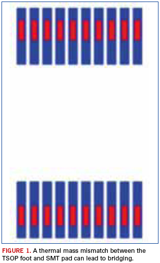
When thermal mismatches are to blame, what’s the cure?
One root cause of bridging with TSOP components is a size mismatch between the TSOP (U2, 24-lead) and the SMT pads. Typically two problems are caused at reflow due to component-footprint mismatch: bridging and insufficient solder volume. Bridging is the result of a thermal mass mismatch between the pad and component lead, and most often occurs with gullwing devices. The foot (toe-to-heel) has a much smaller thermal mass than the pad and heats more quickly in the reflow oven. Molten solder will wet more aggressively to a hotter surface, so the majority of the solder volume pools at the toe and heel and does not evenly coat the pad and component lead. The gullwing lead cannot wet all of the excessive solder volume, and the excess flows off the SMT pad, bridging to the adjacent pad.
Insufficient solder volume is a result of too much surface area for the solder to wet to, and most often occurs with QFNs and RNETs. Since the surface area differences are not nearly as drastic as those with bridging, the temperatures of the SMT pad and the component terminations are much closer during reflow. As a result, solder evenly wets to both surfaces. However, a pad that is too large requires extra solder volume to evenly wet all surfaces and still create a Class III solder joint. Component shortages and substitutions, and poorly designed boards, can cause either, or both, of these problems.
For this board (Figure 1), the bridging with TSOP U2 is the result of a very small foot (red) and a very large SMT pad (blue). The foot length is 0.0246" and the SMT pad length is 0.069". The foot only covers 36% of the pad length. For a properly designed board, the foot should cover approximately 75% of the pad length. The foot is getting much hotter than the pad during reflow, and too much solder volume is pooling at the toe and heel. Solder is flowing off the pad, causing bridging.
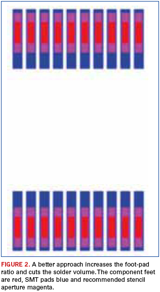
To eliminate bridging, the printed solder volume must be substantially reduced, given the very small component feet and the very large SMT pads. The recommended stencil aperture size is U2: 0.009" x 0.0485" (36% volume reduction).