A new data exchange format, IDX, promises to improve electromechanical design collaboration.
Electromechanical product designers face constant competitive pressure to reduce development costs, improve design cycle times, and eliminate errors that can lead to costly rework. Nowhere is this challenge more apparent than in the integration of PCB layout with mechanical design, where sharing design information efficiently and reliably has long been a bottleneck in the overall electromechanical product design process.
It’s a tough problem to solve. Not only does the shared information have to bridge the 2D to 3D gap, the amount and type of information that needs to be shared varies from design to design and company to company. Plus, the information requirements often change throughout the design process.
For nearly 20 years, the Intermediate Data Format (IDF) has been the preferred file format for exchanging basic design information between the ECAD and MCAD systems that PCB layout designers and mechanical designers use to design electromechanical products. Unlike drawing data formats like DXF and IGES, the IDF preserves design intent during the exchange process, resulting in significant productivity improvements.
But the IDF is not a panacea. Design information that can be shared through the IDF is limited to the board shape, basic component shapes and locations, basic hole definitions and locations, and keep-in/keep-out areas. More significant, IDF files can only represent “snapshots” of the design at any point in time; the IDF does not support incremental changes throughout the design process.
A new data format, known as IDX for “Incremental Data eXchange,” has been developed to overcome the limitations of the IDF and provide a new level of collaboration between board layout and mechanical design.
History of IDX
IDX grew out of discussions between Mentor Graphics and Parametric Technology Corp. and their customers about ways to enable more collaborative use of their respective tools on designing electromechanical products. Faced with the challenges of designing smaller, more complex products, the customers were asking for a design collaboration solution that could not be developed around the IDF.
As a result of these discussions, they engaged the ProSTEP iViP Association, a standards development consortium based in Germany, to develop a new data exchange format for ECAD/MCAD design collaboration and make it available to the entire CAD vendor and OEM community. A project group was established, and work on the new format began in 2006.
The project group created a data model for ECAD/MCAD collaboration called the EDMD (Electronic Data Mechanical Data). The EDMD data model borrows from STEP (Standard for the Exchange of Product model data), an international standard, specifically, Application Protocol (AP) 214 “Core Data Model for Automotive Mechanical Design Processes” and AP 210 “Electronic Assembly, Interconnection, and Packaging Design.” In addition, a goal of the project group was to incorporate the concepts and content of IDF 3.0 in the initial data model.
ProSTEP released an initial version (1.2) of the EDMD in 2008. The current release of the EDMD, version 2.0, was completed and published as “ProSTEP iViP Recommendation PSI 5” in May 2010. The recommendation includes an XML file representation of the EDMD data model. The XML files have an extension of .idx, which is where IDX gets its name.
Some of the key features of IDX that are not found in the IDF are:
XML representation. The EDMD data model is defined with XML schemas, and IDX files are XML documents. This makes IDX flexible and extensible. New features, such as support for etch shapes or traces, can be added in future releases of IDX without affecting current implementations. Plus, XML is familiar to many developers, so there is less reinventing the wheel to support IDX file exchange in their CAD products.
Unique design object identifiers. Every design object has a unique identifier in IDX – not just electrical component instances (uniquely identified by reference designator in the IDF) but holes, keep-outs, mechanical components, and other design objects as well. Unique object identifiers are the key to tracking and managing changes in a collaborative design environment.
Incremental exchange. IDX can represent an initial “baseline” design state, as well as incremental changes to that state and subsequent states. Incremental exchange reduces the amount of design information shared between PCB layout and mechanical design during the design cycle. More important, IDX gives designers the ability to identify what changes are being proposed and evaluate the effect of those changes before accepting them.
Change history. Each design change represented in an IDX file can include a history of who originated the change, when it was made, a comment explaining why it was made, who reviewed the change, whether the change was accepted or rejected, and a comment explaining why it was accepted or rejected. This history is a key element of the collaborative design process.
Inside IDX
The following sections offer a brief look at some of the main aspects of the EDMD data model and how it relates to the IDF:
Geometry. IDX supports the basic geometry of the IDF: polylines (connected sequences of line segments), circular arcs, circles, and composite curves (two or more polylines and arcs joined end to end). Parabolas, ellipses, b-splines, and other curve types are also permitted, although most ECAD systems do not currently support them. The points that define these geometric elements are confined to the x-y plane.
Lines and curves combine to form IDX curvesets. An upper and lower bound can be specified for each curveset, giving the curveset a “thickness” in the Z direction. This is how IDX gives thickness to the board, heights to components, and height-based restrictions on keep-ins and keep-outs. As with the IDF, IDX currently limits geometry to this 2.5D representation because ECAD systems do not generally support full 3D models. However, the EDMD data model supports a full 3D geometry representation for future use.
Shapes. Objects in a board design are created from IDX shape elements. Each shape element specifies a curveset and a type (for example, “part feature” for the board and component parts, and “non feature shape element” for keep-ins/keep-outs). A shape element can be “inverted” to create a void in another shape element. For example, a shape element can be inverted to create a cutout in the board shape.
Shape elements combine to create shapes for the board (called a “stratum” in IDX), assembly components, keep-ins/keep-outs, holes (called “interstratum features”), and other design objects such as mechanical parts. Because shape elements can be combined, it is possible to create board shapes with cutouts, and component shapes with more than one height.
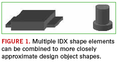
For example, the body of a DIP can be one shape element, and the rows of leads on either side can be additional shape elements. So, although geometry is limited to 2.5D in IDX, multiple shape elements can be used to closely approximate 3D shapes (Figure 1). In the IDF, components only have a single shape.
Items and instances. IDX defines the structure of a board design using items and item instances. Items represent the definitions of board design objects; item instances represent the occurrence of those objects in the board design.
An item can define a single object such as the board itself, a component, a hole, or a keep-out. Or, an item can define an assembly that includes other single objects or assemblies. Each item definition includes all the design information for an object, including its shape, identification and properties, if any. Items can be reused in the design. So for example, an item that defines a component part can be used multiple times in a board assembly.
An item instance is the occurrence of an item in the overall board design structure. Each item instance can include a transformation (currently limited to 2D) that determines the item’s location in the design. Assembly items can contain multiple item instances of single items or other assembly items. This permits IDX to represent hierarchical design structures.
For example, to support panelization as in IDF 3.0, an IDX assembly item could define a manufacturing panel that includes multiple instances of a board part (single item), or multiple instances of a complete board assembly (assembly item).
Roles. IDX extends the concept of ownership in IDF 3.0 with roles. Roles can be assigned to items and item instances to determine who has responsibility for those items and instances, and control who has the right to make changes to them.
Each role specifies a person or group, a type (owner or listener), a category (mechanical, electrical, organizational), a function (design, layout, thermal, etc.), and the item or item instance to which the role is assigned.
For example, with IDX roles, one mechanical designer can own connector locations, and another mechanical designer can own the board shape. The PCB layout group as a whole can own all other component locations.
Properties. In IDX, as with IDF 3.0, properties can be used to assign functional characteristics to component definitions such as capacitance, thermal resistance and power dissipation. Unlike IDF 3.0, IDX extends the use of properties to component instances, shapes, geometry, and most other elements of a design, including the design as a whole. The unit length property, for example, sets the global units for the design.
Properties in IDX can also be used to temporarily extend the functionality of the data model itself. For example, IDX 2.0 does not have an explicit way to represent the side of the board where a placement keep-out applies. Instead, this characteristic of a keep-out is represented as a user property on the keep-out item instance.
Groups. Items can be assigned to groups in IDX, a capability not supported by the IDF. For example, a component can be grouped with a route keep-out. Or, the components that comprise a related portion of a circuit in an area of the board can be grouped.
Constraints can be assigned to a group to determine the behavior of the group, for example, that the items in the group have to move or rotate as a unit. A group can also have an owner that specifies who is responsible for the group.
Text. As with IDF 3.0, IDX provides support for displayable text that can be used to annotate a design but is not part of the design itself. However, IDX allows more control over the size and appearance of text. Each occurrence of IDX text is located within a bounding box defined by upper left and lower right points, and can specify a font, style, weight, alignment, and other attributes.
IDX files are XML documents, so their syntax is XML syntax. The structure of an IDX file is defined by a dozen interrelated XML schemas that comprise the EDMD data model.
Every IDX file contains a root element with a Header section followed by a Body section. The Header contains general information about the file, such as the creator of the file and the tool that was used to create it. The Body section includes all the information – shapes, items, instances, properties, groups, roles, etc. – that describe the current state of the design.
IDX files that represent a complete design state, called baseline files, tend to be large – at least an order of magnitude larger than corresponding IDF files. Large designs can result in IDX files several megabytes in size. However, IDX files that represent incremental design changes are generally much smaller, depending on the number and nature of changes they contain.
Note that IDX files are not designed to be edited by hand. Many of the XML elements in an IDX file contain references to other XML elements in the file. Modifying or removing portions of the file can result in incorrect design information or even corrupt the entire file. IDX files should only be processed by applications that comply with the EDMD data model.
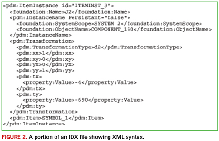
Figure 2 is a small excerpt from the Body section of an IDX file that defines a component instance.\
Managing Change
IDX’s most significant contribution to ECAD/MCAD collaboration is its ability to represent and manage incremental changes throughout the design cycle. This lets designers focus on what’s most important as the design evolves, and collaborate on the changes.
The key to incremental exchange is having unique, persistent identifiers for each design object. With the IDF, only component instances have unique identifiers – their reference designators. In IDX, every item definition and item instance has a unique identifier. So, for example, if a keep-out is removed from the mechanical design and an IDX file is sent with this change, the receiving ECAD system knows which keep-out to remove in the layout by its matching IDX identifier. As another example, having unique identifiers for component instances permits reference designators to be re-sequenced for manufacturing purposes at the end of the design process.
The identifiers are established and communicated in a baseline IDX file exchange. The baseline file sets the initial state of the design and is the starting point for future collaboration. The baseline can come from either CAD system. Often, this is MCAD, where the mechanical designer determines the board shape, mounting hole locations, and the locations of critical components such as connectors and switches. Or, if a new design is based on an existing design, the baseline may come from ECAD.
After the baseline exchange, both CAD systems have the same identifier for every design object exchanged in the baseline, and the mechanical design and PCB layout are synchronized from a collaboration standpoint. Subsequent IDX file exchanges contain only objects that have changed from the baseline or from a later synchronized state of the design.
An IDX change file contains a Changes section that specifies what items and item instances have changed, with references to the actual changes described in the Body section. Changes can result from adding new items (such as placing new components on the board), moving items (such as relocating a mounting hole), modifying items (such as changing the board shape), or deleting items (such as removing a keep-out).
IDX can also indicate the acceptance state of changed items. This allows designers to preview proposed changes and either accept or reject them. The accepted and rejected changes are communicated through another IDX exchange back to the sending system so that the state of the mechanical design and PCB layout can be kept in synch.
A number of CAD vendors now support IDX or have plans to do so. Here’s a quick look at some of them.
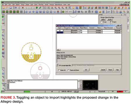
Cadence. Support for IDX is built directly into Allegro 16.5 as a standard feature. Versions 1.2 and 2.0 of IDX are both supported. Importing and exporting IDX files in Allegro is similar to importing and exporting IDF files, including the ability to configure export filter settings (Figure 3). Importing an IDX change file brings up a form that lists all the proposed changes. Selecting an item from the list previews the change in the design so you can see the effect of the change before accepting it. Similarly, when exporting changes, a form is displayed showing all the changes made since the last synchronized state of the design. You can choose which items to include in the IDX change file from this form.
As with the IDF, Allegro also provides a batch executable command for exporting IDX files from the Allegro command line or from an OS command prompt. A batch command for importing IDX files is not provided because importing requires users to preview, accept, and reject changes.
Dassault Systèmes (Catia). Dassault Systèmes is working to implement IDX for its CATIA Circuit Board Design and CATIA Flexible Board Design products. The IDX interface will be implemented by a DS Development Partner, CadCam Design Centar D.O.O.
CATIA currently manages PCB exchanges through IDF 2.0 and 3.0 in CATIA Circuit Board Design and CATIA Flexible Board Design. With CATIA V6, collaboration and synchronization between electrical and mechanical PCB designs is ensured by IDF file sharing. To improve this sharing, IDF files are saved directly within the V6 Platform, ensuring full synchronization at all times, and efficient traceability of design changes.
Dassault Systèmes (SolidWorks). Solidworks support for IDX is provided by the CircuitWorks add-in included with SolidWorks Premium 2012. The CircuitWorks add-in supports both IDX versions 1.2 and 2.0, as well as Mentor PADS .asc files and all versions of the IDF.
CircuitWorks sets up a common folder for exchanging IDX files with ECAD and constantly monitors this folder, sending notifications whenever a new IDX file comes in. If a common folder cannot be set up, CircuitWorks can be configured to automatically email IDX baseline and change files.
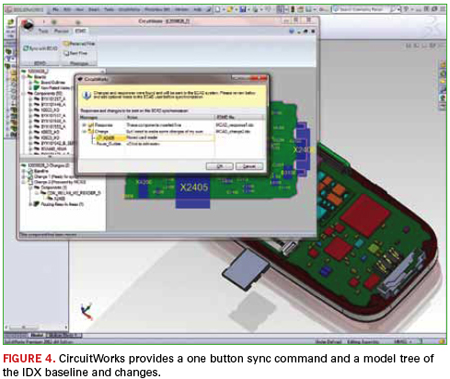
Once a baseline is established and an IDX change file is imported, proposed changes can be viewed and accepted or rejected. A one-button operation updates the SolidWorks design with the accepted changes and exports an IDX change file for synchronizing with ECAD. CircuitWorks maintains a model tree showing the history and status of all changes (Figure 4).
Mentor Graphics. Mentor’s ECAD-MCAD Collaborator (EDMD) supports IDX versions 1.2 and 2.0 for the Expedition Enterprise, BoardStation XE and PADS design flows. The ECAD-MCAD Collaborator provides a 3D visualization environment to review, accept, and reject IDX change proposals from MCAD. Detailed 3D models of electronic and mechanical parts can be imported to help evaluate the effects of the proposed changes. Mechanical packaging data can also be imported so that a complete product assembly with multiple PCB databases can be built completely within the PCB environment.
The ECAD-MCAD Collaborator also allows dynamic view following with the PCB tool. If a part is moved in the PCB tool, the 3D view updates in real time. Panning, zooming and layer display changes in the PCB tools also dynamically update in the Collaborator.
PTC. Creo, PTC’s suite of design software, and Pro/Engineer Wildfire both support IDX.
IDX support for Creo Parametric, PTC’s 3D parametric design app, is provided with the ECAD-MCAD Collaboration Extension (ECX), available beginning with Pro/Engineer Wildfire 5.0. ECX supports both versions 1.2 and 2.0 of IDX.
With ECX, IDX baseline files can be exported or changes proposed for exporting in an IDX change file. One could either manually select the changes to propose from the Creo Parametric assembly or use the compare functionality to propose all changes made since a previous saved version of the board assembly.
When importing IDX files, Creo View ECAD Validate lets you select the proposed changes from a transaction list and preview them in the Creo Parametric assembly. Once it’s been decided which changes to accept or reject in the transaction list, they can be approved to update the assembly and then saved in a new IDX file for ECAD to synchronize the design accordingly.
Creo View ECAD, PTC’s standalone visualization app for ECAD, also supports importing both versions 1.2 and 2.0 of IDX for graphical visualization.
Siemens PLM. NX 8 provides support for IDX through a fully-embedded application called NX PCB Exchange. NX PCB Exchange is developed by Maya Heat Transfer Technologies, an OEM technology partner with Siemens PLM Software.
NX PCB Exchange currently supports baseline IDX version 1.2 transfers. However, NX PCB Exchange also has the ability to compare, preview, and accept/reject changes in IDF files. This functionality will be extended in the near future to support incremental IDX changes. IDX 2.0 files will also be supported.
Zuken. Zuken supports IDX for CR-5000 with the Zuken Interchanger for Creo. As the name suggests, the Zuken Interchanger for Creo is currently optimized for use with Creo Parametric and was developed cooperatively with PTC. Over time, as CAD industry support for IDX matures, Zuken expects to use it with other MCAD systems as well.
The Zuken Interchanger for Creo supports IDX version 2.0 and can exchange both baseline and change files. It also provides filtering capabilities when exporting from CR-5000 so that designers can limit the number and type of design objects included in the resultant mechanical model.
Summary
IDX represents a major step forward in integrating PCB layout and mechanical design permitting collaboration through incremental data exchange. It’s the first ECAD/MCAD data exchange format to provide this capability. As with any new data exchange format, there will likely be implementation issues and missing functionality to resolve over time. The good news is IDX is designed to change and grow as design collaboration needs evolve. A critical mass of CAD vendors now support IDX, so the first test of a standard – acceptance – has been met. Many vendors have committed significant time and resources to develop their IDX-based collaboration solutions, and they want these solutions to work for their customers.
Dave Kehmeier is an MCAD/ECAD integration consultant and developer of the IDF (liaiseintegration.com); This email address is being protected from spambots. You need JavaScript enabled to view it..
Start at the finish: the event that signaled the failure.
Question: I have a product that has failed, and we have traced the failure to an open in the flexible circuit. The flex circuit shows no obvious visible indications of the failure. We would like to further understand why the flex circuit has failed. What steps should we take in our failure analysis of the flex circuit?
Answer: Surely you jest! Flex circuits never fail!
OK, you got me. As much as I would like to say that flex circuits are immune to failure, they are in reality prone to many of the same problems that can cause issues on rigid PCBs. In addition, the very nature of a flex circuit being required to bend and flex introduces a host of other mechanical issues that can cause problems. So where do you start?
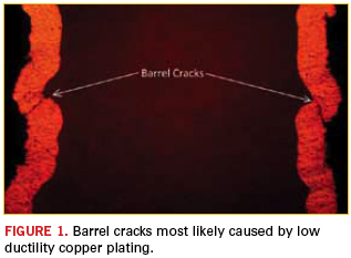
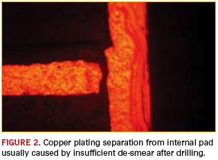
First, ask if the part failed after a particular event, such as being exposed to highly elevated temperatures, thermal cycling, shock and vibe, or repeated flexing. The event that signaled the failure usually will give a good indication of where to look for the assignable cause of the failure. For instance, if the failure occurred after any type of thermal excursion or cycling, first examine the plated-through holes or blind vias for barrel cracks or plating separation from the hole wall (through holes) or landing pad (blind vias). Barrel cracks are typically the result of insufficient copper plating thickness, or poor copper plating ductility and/or tensile strength.
Separation is usually caused by inadequate etch back (smear removal) from the drilling processes. Isolate the plated holes on the faulty net and perform a cross-sectional analysis of these holes. Always ensure that you thoroughly polish and micro-etch the sample mount prior to examination. The cracks or separation you are looking for may be only 0.0001" wide and easily smeared over by the soft copper during polishing. If the sample mount is not properly micro-etched, the cracks or separation will not be visible. In a properly polished and micro-etched mount, the copper should have a dull, grainy appearance (not shiny), and there should be a clear line between the base copper and copper plating on the top and bottom surfaces. If the failure seemed to be a direct result of thermal activity, there likely will be visible cracks (Figure 1) or separation (Figure 2).
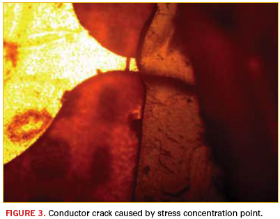
If the event that triggered the failure was a flexing operation, start with a thorough visual examination using a microscope on the areas that are flexing. Look for anomalies in the cover material (such as ripples) that can indicate a potential problem with the conductors below. Also, look carefully at the flexing area for features that could be stress concentration points (e.g., conductor width or directional changes, openings in the cover material, or terminations of platings or coatings). Any of these features in a flexing area can be a recipe for disaster. Once suspect areas have been identified, increase the microscope magnification and carefully inspect for cracks. Again, the cracks you seek will usually be very small and may appear to just be a line across the conductor. Figure 3 illustrates an excellent example of what not to do in your design. Notice how the narrow conductor is exposed for a very short length. This conductor was also plated with nickel/gold, which is another no-no in an area that may flex. Nickel plating is very brittle, and even a small amount of flexing can cause a crack, which will then propagate through the entire conductor thickness.
If the circuit has soldered connectors, sockets, or pins and failed after shock or high vibration, carefully inspect the solder joints. This inspection should be performed using a microscope at moderate magnification. Start by looking for any solder joints that may have been questionable to begin with, and expand to other solder joints if the initial search does not reveal anything. Look particularly for cracks or separation between the solder and the pin or pad.
Virtually all flexible circuit failures are a result of either thermal or mechanical stresses. Once the type of stress that triggered the failure is identified, focus the investigation on the circuit features that would be the most affected by that type of stress. And as always, if you “hit the wall” in the failure analysis, do not hesitate to contact the flexible circuit manufacturer for guidance. Chances are they have seen it before and can save you some sleuthing time.
Mark Finstad is a senior applications engineer at Flexible Circuit Technologies (flexiblecircuit.com); This email address is being protected from spambots. You need JavaScript enabled to view it.. He and co-“Flexpert” Mark Verbrugge (This email address is being protected from spambots. You need JavaScript enabled to view it.) welcome your questions.
First stage of a three-phase test plan is successfully completed.
Whenever a new technology is discovered, someone has to be first to try it. The PCB design and manufacturing business in particular expends a great deal of time and money to refine a process based on a new technology. Someone has to work out the kinks, discover misplaced assumptions, experience delays in first manufacturing runs; the list goes on. But when someone is the first to succeed, everyone learns by example – that is, if the initiator is willing to share their experience.
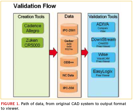
The IPC-2581 Consortium was organized by a group of companies committed to promoting the IPC-2581 standard for industry-wide adoption of an open, global, neutral format for transferring PCB design data to manufacturing. Within the IPC-2581 Consortium, a technical work group was created to validate the accuracy and completeness of IPC-2581 data produced by PCB CAD vendors. This group comprises a good cross-section of industry leaders providing expertise in the various domains that the IPC-2581 standard will support.
The first activity of the technical work group was to create a validation plan based on the three major areas of PCB production: bare board fabrication data, assembly data, and test data. Once the plans were put in place, an aggressive schedule was set for each of these three phases.
The first phase of the test plan was to validate bare-board fabrication data contained within the IPC-2581 single-file format. Phase I testing compared the IPC-2581 fabrication data against today’s existing export data formats (artwork, NC drill and NC route) for accuracy and completeness. Cadence and Zuken provided initial test cases from internal designs, followed by real design data from IPC-2581 Consortium members NVIDIA and Fujitsu. Tools provided by ADIVA, DownStream Technologies, EasyLogix, and Wise Software consumed the IPC-2581 data and ran comparisons against the artwork, drill, and route data.
At IPC Apex Expo in February, the IPC-2581 Consortium’s Technical Team was pleased to announce successful completion of Phase I, and demonstrated its progress to the IPC-2581 Standards Committee. Samples of the test data in IPC-2581 format can be downloaded from the Consortium website at ipc-2581.com.
DownStream Technologies, EasyLogix and Wise provide free viewers (which can also be downloaded from the Consortium website) to view the sample design data. The IPC-2581 Technical Team is diligently working on the next phases of validation – defining the details of required data, validation of that data, and working with the tool developers that will create and consume IPC-2581 data.
The IPC-2581 Technical Team also provides another benefit to the standard by identifying enhancements and new technology to be considered for adoption into the IPC-2581 standard. As the Technical Team continues to collaborate, we have a strong voice for the development and growth of the standard to meet the ever-changing challenges of the PCB and manufacturing industry.
Consortium membership, now at 27 companies, is growing with recent additions such as Polar Instruments, Qualcomm, Velux and Screaming Circuits. By sharing our experiences and our findings, the IPC-2581 Consortium is paving the way to broad adoption of the standard throughout the PCB community.
Visit the Consortium website to see the progress of the validation project. More important, join this design and supply chain company–based Consortium to support an open, neutral, global standard for efficient PCB design data transfer to manufacturing.
Edward B. Acheson is product engineer at Cadence Design Systems (cadence.com); This email address is being protected from spambots. You need JavaScript enabled to view it..
Gazing over the scenic San Diego harbor, more than a thousand people gathered at the Electronic Components and Technology Conference (ECTC) to discuss cutting-edge developments in electronics packaging, materials, and assembly.
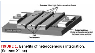
While crowds gathered for the numerous 3D through-silicon via (TSV) papers, an equal number of attendees focused on interposers – a solution that appears more near term. Papers from Altera, Cisco and Xilinx focused on product introductions and plans with silicon interposers. In an interactive session, Xilinx discussed its latest product, a 2.78Tb/s FPGA with serial connectivity – a heterogeneous solution combining three 28nm FPGA slices, two 40nm electrically isolated 28F transceiver devices, and 13G transceivers on a 65nm passive interposer (Figure 1). Cisco described a future solution featuring memory and logic on a passive interposer, while Altera’s solution will take advantage of TSMC’s chip-on-wafer (CoW) technology.
Remarkably, the structures look similar to what the industry called MCM-D or multichip modules (D is for a deposited thin film dielectric) more than 15 years ago. The major difference is that today’s interposers have TSVs, but some issues, such as ensuring a high-yield process is used to produce the substrate, mounting known-good die, thermal issues, and infrastructure, have not changed. Several companies discussed the possibility of using glass interposers and some discussed use of a laminate substrate with fine features instead of a glass or silicon structure.
The quest for 3D TSV. While 3D-TSV structures planned for immediate commercial production remain elusive, several presentations provided insight into structures on the horizon. Research institutes, including CEA LETI, various Fraunhofer organizations, IME, IMEC, ITRI, KAIST, RTI, and others, provided details of research underway.
Texas Instruments provided a look into its development work on an analog application with TSVs in a wafer-level package structure. Image sensor developments from CEA LETI and research partners NXP and ST Microelectronics showed a path from backside vias due to stacking in future image sensor applications.
GlobalFoundries CTO Gregg Bartlett provided one of the most compelling arguments for 3D TSV adoption during his luncheon keynote: the cost of future lithography systems for next-generation silicon node technologies, which tops $100 million. The promise of 3D TSV, with its advantages of improved interposer, bandwidth and latency, is as enticing as the vision of a harpy to a lost mariner – her cries drawing him into the jagged rocks near the coast. Whispered in the hallways during the conference were the trials and tribulations of the debond step in the wafer thinning process – required for both silicon interposers with TSVs and 3D TSV stacks. A number of material developments hold promise, but the peril of impact on yield remains.
Coreless substrates. Coreless substrates appear to be becoming a reality. A special evening session focused on advanced coreless substrate and material technologies from Japanese companies. Between sessions several substrate makers confirmed that demand for coreless substrates is increasing, and Intel provided details of its developments with a coreless substrate with controlled warpage – one of the big concerns that has slowed adoption of the structure.
Crowds jockey for a seat in Cu pillar sessions. Attendees crowded into standing-room-only presentations that focused on copper pillar developments. Presentations from foundries, OSATs and other companies clearly indicated the technology is becoming mainstream for more than just Intel. ASE, Amkor, STATS ChipPAC, SPIL, PTI and others discussed assembly progress. TSMC, now also playing the part of an assembly service provider, instead of just a foundry with bumping capability, provided a peak into its activities with Cu pillar.
Fan-out wafer-level packages (WLPs), embedded components, LEDs, MEMS and alternatives to gold wire bonding captivated the interest of attendees. Many new material developments, especially related to underfill, were presented. Discussions of pre-applied underfill from materials suppliers and companies with applications were numerous. Increased use of Cu pillar appears to be one of the major drivers in the introduction of nonconductive films and pastes, with multiple presentations on the new formulations.
Planning is underway for next year’s ECTC, to be held in Las Vegas next May. Abstract submissions are due in October (ectc.net).
As China matures, a host of factors could rebalance the geographical supply chain.
Nearshoring and reshoring are significant topics of discussion in the outsourcing community. Factors that led China to become the world’s workshop are shifting. China’s labor costs have doubled in the past two years and will likely grow another 15% to 20% in 2012. Some OEMs are simply looking to move business to other countries in Asia. Fuel costs and recent natural disasters are key reasons why many are looking closer to home to lower their risk with shorter supply chains. Tighter credit is making inventory buffers more expensive to maintain. All this has led Boston Consulting Group to predict that by 2015 the percentage cost differential between China and some parts of the US will be in the single digits.1
As few as five years ago, those without an “Asia plan” risked being left behind. Today, OEMs that lack a nearshoring strategy are the ones that risk falling behind. At Spectrum Assembly, we see many companies starting to evaluate the true cost of nearshoring vs. offshoring, particularly with high-mix projects. A Pennsylvania State University study found that most companies took a fairly unsophisticated approach to analyzing offshore sourcing costs.2 The key is balancing tangible landed cost against risk factors that are hard to put into dollar amounts. We see several cost and risk factors routinely overlooked in initial cost evaluations. What are the potential cost impacts to evaluate in each of these areas?
Regulatory supply base constraints. Products in highly regulated industries may have very limited supply base options relative to certain components. For example, one of our customers whose products were used in the nuclear industry could use only raw cable that met very rigid industry specifications. The only two suppliers of that type of raw cable were located in the US. An offshore build required shipping raw cable to China, assembling the product and then shipping it back to the US. Add air freight costs to support demand variations of a build-to-order product, and a US build was clearly the most cost-effective option.
Intellectual property theft risk. IP theft is always a risk in certain geographies. Variations in IP laws between countries can make IP violations expensive to prevent. Litigation is expensive wherever you are. Lost market share can be difficult to regain. For products that will be sold in the countries in which they are manufactured, this is simply a cost of doing business. However, if the product will not be sold in that region, the costs of maintaining IP protection in that region should be evaluated.
OEM team time and travel costs. Fit between teams is an important part of a successful outsourcing relationship. The level of product maturity and project complexity dictate how much time sourcing, engineering and contractor teams need to spend together. The cost of deploying teams at a distance, extended work hours to support multiple time zone teleconferences and potential language or communications issues should be considered in a total cost evaluation. Another driver is preference for the convenience of a local supplier when significant engineering interface is required.
Quality concerns. Most OEMs audit to ensure an offshore contractor has acceptable levels of quality. Contractors in these regions are used to substituting wherever they can to reduce cost or keep lines running, and on-the-fly AVL changes are common. If the contractor isn’t watched, unauthorized substitutions may be inadvertently made. This can create significant issues for companies in regulated industries such as medical equipment or in any mission-critical product that requires third-party design approval or registration. Quality issues can creep in over time, particularly in high-mix projects. As a labor market matures, personnel turnover increases. This in turn drives learning curve quality issues as replacement personnel are hired and trained. A factory in China can experience turnover of upwards of 80% season to season. The standard training strategy with a high turnover workforce is to train them well on a specific task with few product options. Comparatively, onshore companies focus on developing low turnover workforces through pay-for-skills programs, and lower labor costs by using fewer employees to perform a wider variety of tasks. As an example, over 50% of our production operators have been with Spectrum Assembly more than a decade.
Alignment with contractor’s business model. Two dynamics are changing the model in Asia. First, internal demand is causing China to go up market. Simple jobs are being no bid in favor of more challenging work with more value-add. Second, the recent disasters in Japan and Thailand drove offshore contractors to implement disaster recovery plans and prioritize work for their most important customers. The OEMs whose production was delayed in favor of contractors’ larger customers are now looking for partnerships with contractors who see them as a fundamental part of their business strategy.
Expedited shipping costs driven by demand variations. Another challenge is that demand is hard to forecast. Most top distributors will say that in North America the mean average deviation (MAD) on a 30-day horizon is not much better than 50%. As a result, OEMs with higher mix product lines have greater schedule flexibility if they assemble locally with an onshore contractor and a Lean supply base philosophy where variations can be addressed fairly easily. With an offshore pipeline, variations may trigger air freighted shipments. One or two overseas premium air shipments can completely cancel out any labor savings.
Resource opportunity costs. The first benefit that most OEMs look for to justify an outsourcing project is the variable cost savings embodied in landed price. When offshore and onshore pricing is near parity, resource opportunity costs need to be carefully analyzed. For example, longer pipelines driven by sea shipments increase the potential inability to meet varying customer demand. Onshore suppliers reduce or eliminate team travel time and usually require less oversight than offshore suppliers. Time zones are more compatible to normal working hours. In short, there is a significant savings related to non-value-added time spent on the project when a domestic partner is used. Eliminating that non-value-added time frees those resources. From an inventory perspective, working capital is reduced or can be redeployed in ways that increase a company’s ability to respond to variable demand. From a personnel standpoint, team members can be redeployed to next-generation product development or launching entirely new product lines.
Nearshoring is not right for every product. However, focusing on these cost drivers can help identify products that would benefit from this strategy. All labor markets eventually mature and increase in cost. A strong offshore/nearshore total cost analysis process is critical in ensuring that sourcing teams make the most cost-effective decisions.
References
1. H. L. Sirkin, M. Zinser and D. Hohner, “Made in America, Again. Why Manufacturing Will Return to the US,” Boston Consulting Group, August 2011, p. 3. 2. R. Young, P. Swan, E. Thomchick and K. Ruamsook, “Extending Landed Cost Models To Improve Offshore Sourcing Decisions,” International Journal of Physical Distribution & Logistics Management, vol. 39, no. 4, 2009 p. 320.
The 42nd International Electronic Circuits Exhibition was held June 13 to June 15 at the Tokyo Big Sight in Japan. The three-day event is the largest trade show for the printed circuit industry, and included the following related exhibitions: JIEP (26th Advanced Electronics Packaging Exhibition), JISSO PROTEC (14th JISSO Process Technology Exhibition) and the Large Electronics Show 2012. Two new events added to the show were Monotsukuri Fiesta (Manufacturing Festival) and the 1st Printed Electronics Convention. Additionally, there were many special seminars and poster sessions that targeted both the novices and the experts.