A unified front might be the trick to obtaining a fair price.
While it could be said that our industry, steeped in a tradition of phenomenal technological breakthroughs, has done some really fantastic things over the years, one thing that we have collectively failed miserably at is conveying the value that the design, fabrication and assembly of printed circuit boards provides the end-user. Worse, I question whether we even know how to measure the true cost of the value we bring to our collective customer base.
What is “value?” I view value – total value – as the sum of all parts that go into providing a product. The sum of all the parts includes not only the materials and supplies that make up a product, but also the competent and innovative people, regardless of academic background, who actually make it, and the investment in the best available equipment – which does not necessarily mean the newest. Equally, the sum of the parts includes the oft-forgotten but essential “little things,” like commitment to adequate inventory, training staff on new processes and methods, and servicing customers that all too often need considerable hand-holding to understand the options available to get what they are ultimately asking for – all with exceptional quality, delivered quickly and on-time.
Collectively, we have been mediocre at best at explaining (read: selling) this value. Trade groups have failed to broach head-on a meaningful discussion of the value our industry collectively provides to end-customers. Ditto for the supply base. Worst of all, the individual companies aggressively tout their abilities but don’t connect the dots in terms of how their products and services really benefit end-customers. Rather than marketing the value that goes into the design and manufacture of PCBs, each company will discuss in vague generalities why they are better than the others, or how they can save the end-customer some money on the next order. Rarely do any of us tell customers that collectively we all provide significant value, and therefore, with all due respect Mr. Customer, we all should be valued!
Why tell a customer that everyone – not just your specific company – is of value? Because only by selling the value of all companies will any company be able to command what they are worth in the marketplace. Customers hear only the bean-counter mantra that we all are just commodities. Instead, customers need to hear that, regardless of our location, niche or size, we are all providing true value, are worth the price we charge, and perhaps they, the customer, should pay more attention as to whom they buy from, and why.
This is not about fixing prices or other collusion but rather presenting a unified front to promote what we all apparently take for granted: that there is real value to what we do. We as an industry – associations, suppliers and manufacturers – owe it to ourselves and each other to educate customers on that value, and that value needs to be reflected in a fair price.
A fair price also requires understanding, valuing and charging based on the accurate cost of product development and manufacture. Rather than incorporating the total cost into a price, we fall victim to competition, real or perceived. How often do we complain about the renegade “bucket shop” or “big company from wherever” that drops its price so “none of us” can make money? Maybe instead we should remind customers that those who drop prices just to fill their plant have more often than not failed, leaving customers stuck with no product.
Possibly a better approach would be to add to our sales presentations the value our products and services provide, and explain the total cost that goes into each job processed and manufactured. Equally, maybe in little ways we can all, together, reinforce that true value is being provided, and not capitulate when customers demand unrealistic price targets or extended payment terms “like the distributors accept.” None of us are distributors; we build to print and purchase specific materials processed per specification and, therefore, have total costs that go into providing true value. If everyone holds their end up, the message will get across! This is not for the faint of heart. Make no mistake, customers love when an industry works together, by plan or by accident, to create a downdraft in pricing. In fact, customers encourage this by convincing suppliers that what they provide is of little or no value. And when this happens, regrettably too often we as an industry capitulate. Yes, some may resist, but a chain is only as strong as its weakest link. If one firm breaks ranks, we all suffer.
Long-term, to remain viable, we need to do a better job conveying how much value we all, together, provide customers. This requires a multifaceted approach. Yes, we need to continue to explain our technology and service. However, we have to expand on that to include the true cost of providing ever-improving service and investing in cutting-edge technologies. Equally, we need to better communicate the outstanding technical competence required of employees throughout the industry. Circuit boards and all they go into are not designed, fabricated or assembled strictly by machines. Skilled people make it happen, and that is a core value – and true cost – too often ignored or undervalued by end-customers, and rarely effectively communicated by our industry as a differentiator.
Our industry has a tradition of being innovative. Clearly our companies have excelled as technology leaders. Isn’t it time that, together, we fashion a message that all the companies that provide the leading edge technology that end-users have come to expect are providing true value?
Consolidation has been occurring for years in the electronics supply chain, and distributors have been no strangers to the phenomenon. In fact, just over a month ago we interviewed David Wolff, founder and president of P.D. Circuits, a major US-based bare board broker that was being acquired by NCAB Group of Sweden.
So when the news broke on Sept. 26 at PCB West that P.D.’s main US competitor, Bare Board Group, was putting together a deal of its own, it seemed part of the normal fare.
But when it was revealed just whom BBG was buying, the picture became a lot more interesting.
BBG’s acquisition target was Hunter Technology’s printed circuit board fabrication operations. The move dramatically changes the distribution landscape because, for the first time in years, a major regional distributor will also have internal manufacturing capability.
Although rare these days, the manufacturer-distributor model isn’t a completely foreign concept, but it’s more commonplace among contract electronics assemblers. No fewer than five firms in the CIRCUITS ASSEMBLYDirectory of EMS Companies offer some degree of component or equipment reselling. Most are small. Jaco Electronics in New York offers name-brand flat-panel displays, but also performs some degree of CTO box-build and assembly. T-Tech Electronics in Penang distributes components and offers EMS services. STI in Huntsville, AL, is a Tier IV EMS and reps various equipment lines. In January, electronic components manufacturer AirBorn acquired EMS firm AESCO Electronics.
Others have tried on a larger scale and failed. After acquiring contract assembler Hibbing Electronics in 1998, components disty Reptron’s sales quickly peaked, topping $300 million. Within five years came a reorganization. After two more years of repeated losses, it was sold to Kimball. In 2005, when EMS firm Rad Technologies acquired a distribution operation, it had the goal of reaching $100 million in annual sales within the year. It, too, is now out of business. Even fewer component distributors have attempted to broker bare boards. When we researched the market a few years ago, we found only one company – Elfa, in Sweden – offering PCBs on its line card. More typical is an arrangement whereby a disty links its website to that of a fabricator’s, thus simplifying the board buying process. A year ago, for instance, element14 did just that through partnerships with PCB manufacturers Sunstone Circuits and Pentalogix.
A few months back, PCB distributor Fineline Global announced a 25% stake in Shenzhen Fastprint Circuit Tech. What’s less clear, however, is whether Fineline is doing more than simply investing in the fabricator.
That’s why BBG’s move represents a more significant undertaking. Distributors have traditionally shied away from product build because the two models require different sets of business practices. Inventory turns are valued in both industries, of course, but outsourced manufacturing emphasizes service over commoditization. PCBs are not off-the-shelf parts; each part number is a unique design. And then there’s the conundrum of how the disty keeps its other circuit board suppliers happy, while also maintaining its own loaded factory. BBG is novel in trying to cross that bridge.
But there’s a tempting potential payoff. PCB distributors are now pushing into the $100 million realm, which would be big enough to make Dr. Hayao Nakahara’s NTI-100 list of the largest board fabricators (which we published in September). NCAB’s acquisition of P.D. puts it up against that magic revenue number.
The Hunter deal won’t get BBG there, not by a long shot. Privately held Hunter doesn’t report revenues from its fab operations, but they likely aren’t higher than $4 million a year. BBG’s annual run rate is about $30 million.
Still, as BBG founder and president Greg Papandrew told me years ago, the one disadvantage he always faced selling against bricks-and-mortar board shops was not having what he called the “storefront.” Apple sold lots of iPhones and iPods through the traditional channel, but things really took off when it opened its own retail stores. Sometimes, customers just want to feel close to the original supplier.
To be sure, almost every US- or Europe-based fabricator also brokers boards. IPC data indicate close to one-fifth of the boards sold in the US by domestic fabricators were purchased from offshore sources. So BBG will be up against not only the dedicated disty competitors, but also an army of small shops – most roughly the size of Hunter – which already have overseas partners.
In the end, the model itself is less important than the execution. If BBG, or others that follow in its footsteps, can continue to get reliable PCBs into the hands of customers on-time and on-budget, this will look like a brilliant move. And if not, it won’t.
Abstract: In this study, an accelerated test condition [130°C, 85% RH, and 100V DC] was used to investigate conductive anodic filament (CAF) in two organic package substrates: 1) cyclo-olefin polymer–glass fiber composite (XR3) and 2) epoxy-glass fiber composite (FR-4). Test coupons with through-via spacing of 100µm and 200µm were investigated. CAF failures were not observed in either substrate type with spacing of 200µm. With spacing of 100µm, insulation failures were observed in FR-4, while XR3 exhibited stable insulation resistance during the test. The substrates were characterized using gravimetric measurement, and XR3 was found to exhibit significantly lower moisture absorption compared with FR-4. CAF failures in FR-4 were characterized using scanning electron microscopy and energy-dispersive x-ray spectroscopy. Results suggest a strong effect of moisture sorption of organic resins on CAF failure at smaller through-via spacing in package substrates. (Journal of Electronics Materials, November 2012)
PCB Substrates
“Data Mining for Creep Corrosion on Desktop Computers”
Abstract: When the PC industry switched from traditional leaded (SnPb) solders to lead-free (SnAgCu) solders, the industry considered new board surface finishes as well. The corrosion resistance of the leading Pb-free coatings, immersion silver (ImAg) and organic solder protectant (OSP) were questioned. With several years of field experience, organizations can quantify the efficacy of ImAg and OSP with actual field data. For the past few years, Intel’s warranty return centers performed a visual inspection for corrosion on all motherboards returned. A statistical analysis was performed on all returned products to determine the general extent of corrosion and to look for subpopulations with statistically significantly higher and lower return rates. It was found that excessive flux application dramatically affected the corrosion incident rate for motherboard products with ImAg finishes. No correlation existed between the percentage of sales to particular countries or geographies and the relative corrosion incident rates for the desktop motherboard part numbers in the study. Newer motherboard part numbers with OSP coatings experienced significantly reduced incidents of corrosion compared to earlier motherboards with ImAg coatings. Components on desktop motherboards showed no obvious signs of creep corrosion in the warranty returns population studied. (SMTA International, October 2012)
Solder Joint Reliability
“Characterization of Stress–Strain Response of Lead-Free Solder Joints Using a Digital Image Correlation Technique and Finite-Element Modeling”
Authors: G. Khatibi, M. Lederer, E. Byrne, A. Betzwar Kotas, B. Weiss and H. Ipser
Abstract: The stress-strain response of miniaturized Sn-Ag-Cu (SAC) lead-free solder joints in the thickness range of 80µm to about 1.1mm was studied. A high-resolution 3D digital image correlation system was used for in situ measurement of displacement and strain fields in the solder joints during tensile testing. These measurements showed that the localization of plastic strain and stress buildup occurs mainly at the interface of the solder. With increasing solder gap thickness, the size of the plastically deformed zone in the solder increases, resulting in transformation of a brittle interfacial fracture to a ductile fracture within the bulk of the solder. The experimental deformation plots of solder joints and strain-rate-dependent tensile tests on bulk solder material were used to establish a new constitutive material model for the solder. This strain-rate- and pressure-dependent material model was implemented in ABAQUS through the user subroutine CREEP. In agreement with the experiments, the finite-element method simulation revealed a pronounced thickness effect leading to higher tensile strength of thinner solder joints. (Journal of Electronics Materials, November 2012)
“Reliability of Passive and Active Components with Differences According to Lead-Free Paste Characterization”
Abstract: Components were analyzed according to shear stress and solder joint cracking. The study compared different flux and solder paste formulations in terms of wetting properties, void formation and reliability results for active and passive components. For passive components, pure nickel and tin finishes were compared. Shear stress was analyzed under automotive requirements. Test conditions used in the testing procedure were temperature cycling with different parameters in terms of deltaT: -40°/+125°C (30'/10"/30'). Data are available for 2000 cycles. Active components were also tested with this procedure. These components had different finish terminations, such as tin and NiPdAu/Ag for LQFPs, and eutectic SnAg and SAC balls for BGAs. Analysis was performed by cross-section and crack length after cycling measured. (SMTA International, October 2012)
This column provides abstracts from recent industry conferences and company white papers. Our goal is to provide an added opportunity for readers to keep abreast of technology and business trends.
Why we need a rapid prototype model where the end-product is “grown,” not built from disparate parts.
I’ve been working in the electronics product design and fabrication industry for 18 years, and over that time I’ve seen a lot of technology evolve. The resounding issue that occurs to me every time I implement DfM or DfT techniques in a new design (I do about 130 a year) is the true lack of integration of manufacture with regard to the mechanical packaging of electronics products and overall function.
My colleagues grow weary of my incessant emoting concerning the need to move from planar PCB fabrication and subsequent tedious mechanical mounting of components, subsequent interconnection and packaging, and the disparate steps involved in final assembly of a product toward a fully intrinsic/monolithic approach – one based on techniques such as those used for rapid prototyping of mechanical parts, similar to fused deposition modeling (FDM), whereby a device is a true intrinsic unit basically grown from the various materials required for form and function.
For example, instead of purchasing individual components such as tantalum capacitors, one merely purchases the raw tantalum compounds, licenses the fabrication formula from, say, Kemet and integrates this into what I describe as a “liquid chain,” one in which all materials in their raw form are combined on a molecular level to grow the desired product. This includes all the semiconductors/conductors, other passives, displays, and so on, which are enveloped in the housing materials. As in FDM and stereolithography (SLA), this could be a layered process combined with other processes analogous to those now used in pure semiconductor fabrication.
I use tantalum capacitors as an example because, a few years ago, there was what many trade publications deemed “a shortage of tantalum capacitors” that was incorrectly attributed to a shortage of tantalum. I knew some people associated with the Kemet factory in North Carolina and called one up, mentioning what I had read. He unequivocally stated that his facility currently had plenty of tantalum material in storage bins, the issue being one where he was unable to get the computer-controlled machinery required to make the actual parts. I jokingly suggested that it might be possible that the manufacturer of this specialized equipment wasn’t able to allocate enough tantalum caps from their distributor/supplier, as they were a bit of a niche buyer. Long silence on the other end of the phone followed.
Another issue is that if you look at the amount of material waste in just packaging printed circuit board components for shipment and delivery to EMS facilities for use on automated pick-and-place machines, the advantage of a monolithic approach is very apparent. Just look at any TI datasheet; at least three pages are devoted to reel/tube orientation and packaging, materials that themselves have to be tooled and eventually are discarded (or hopefully recycled), enveloping more mass, process and time than the actual component fabrication itself.
A distinct advantage in striving toward monolithic methods is the apparent advantage in high-speed and RF/wireless design, where as a designer, I now can use a 3D space for interconnection of controlled impedance waveguides, instead of being limited to a simple 2D planar approach trying to fudge microstrip and stripline topologies into a working subsystem that will still be fraught with failure due to interconnect processes, thermal issues, and subsequent issues involved in using soldering processes that really haven’t changed since the early 1950s. And now with the problems created with the higher reflow temperatures required for processes needed to comply with RoHS initiatives, as outlined by Dr. Howard Johnson and others at NASA1, further refinement of current production methods is just simply putting a Band-aid on a broken leg.
With some modification, current EDA and parametric mechanical software tools could be tailored to provide post-processing for these fabrication techniques, but with considerable advantages over the current methodology that relies on distinct and discrete fabrication steps – chip/passive component fabrication, PCB fabrication, mechanical tooling and fabrication – resulting in a much tighter, more efficient production process with a significant decrease in environmental impact, less waste, and much higher yields.
Imagine your cellphone as being a single block of function, with a minimum of custom components, replacing all mechanical actuation with touchscreens (as is already being done), with no need to use all these secondary operations for sub-assemblies. This is what we need to strive for.
We’re heading toward another “tyranny of numbers,” similar to the one Jack Kilby faced when presented with silicon micro modules, a situation that led him to design the first monolithic IC chip.
References
1. Howard Johnson, “Rolling Back the Lead-Free Initiative,” High-Speed Digital Design Online Newsletter, vol. 10, no. 1, sigcon.com/Pubs/news/10_01.htm.
Wayne Mitzen is a cofounder of Fast Product Development (fast-product-development.com), and holds US patents for RF devices, imagers and wireless intrusion detection systems; This email address is being protected from spambots. You need JavaScript enabled to view it..
Question: What is the difference between a flexible circuit and a membrane circuit? Are they both considered flexible circuits? How do I know which to choose for my application?
Answer: Historically, the term “flexible circuit” or “flex circuit” has implied a circuit with photo-etched metal conductors (generally copper) on a film substrate (generally polyimide). Many of the manufacturing processes involved in building flexible circuits are very similar to those used in manufacturing rigid printed circuit boards. The main difference is that virtually all the insulating and bonding materials used to make flexible circuits are much thinner and generally unreinforced (films), as opposed to the glass-reinforced laminates used to construct rigid PCBs. The term “membrane circuit,” on the other hand, typically refers to a circuit that has printed conductors (usually screen-printed) formed using conductive inks. Membrane circuits are created using additive processes, whereby all conductive and insulating materials are added in layers to the base material. Many conductive inks can be used to create the conductive patterns, but most rely on silver as the conductive component. The base insulating materials that membrane circuits are printed onto are typically polyester films.
Determining which of these variants is best really depends on the application and how the circuit will be processed and used. The decision to use membrane circuits is typically driven by cost. Polyester materials are much less expensive than polyimide, and the cost of forming silver ink conductors is significantly less than the photoetching process required to form copper conductors.
However, with reduced cost come many significant limitations. Polyester materials cannot tolerate the high temperatures that polyimide can withstand. For this reason, the upper service temperature will be limited to under 105˚C with PEN, and even lower with other polyester materials. When screen-printing conductors, it is not possible to define features as small as can be done with photo-etching. For this reason, the wiring density of membrane circuits is significantly less than photo-etched polyimide/copper flex circuits. Connections to connectors and SMT components are typically limited to ZIF style connectors, insulation displacement contacts, or silver ink in lieu of solder to attach components. Silver conductors are designed to handle small signals, so electrical current must be limited to 100 MA or so. Last, the additive processes used to create a membrane circuit limit the construction to a just a few layers. The vast majority of membranes in use right now are just one or two layers, with a very small number that add another two to three layers. Since it is not possible to use copper plating to interconnect layers, the layer connections are made by forming openings in the dielectric layers that permit the conductive ink from one layer to connect to the layer above or below.
As stated, copper/polyimide flex circuits are more expensive than polyester membrane circuits. But with the added cost come additional improvements in capabilities and performance in some important areas. For instance, most flex circuit manufacturers can easily make copper/polyimide circuits with 8-plus conductive layers. In addition to the extra layer capability, many vendors can supply circuits with conductor widths and spaces that are well below 5 mils. This results in the ability to pack much higher wiring density into the same amount of space as a comparably sized membrane circuit. If even higher wiring density is required, the flex circuit manufacturer can move to a rigid-flex design, permitting the layer count to increase to 20-plus conductive layers. (Caveat: 20-plus layer rigid-flex circuits are really expensive.) The other significant benefit of copper/polyimide flex over a membrane circuit is a much higher temperature rating. While a flex circuit will not tolerate temperatures as high as those a rigid PCB is capable of, they can withstand soldering temperatures for short periods of time. This permits connectors and components to be assembled using standard pick-and-place and reflow equipment to populate the circuits. And copper/polyimide flex circuits can operate for extended periods at temperatures well above what a membrane circuit can tolerate. Finally, copper conductors can carry vastly more electrical current than similar-sized silver conductors.
When weighing options in choosing your flexible interconnect, consider cost and also performance factors to determine the best fit for your application. Membrane circuits and copper/polyimide circuits occupy their own unique niches in electronics interconnection. Choosing the right one for your application will ensure the best overall value. As always, do not hesitate to contact your friendly neighborhood flex circuit (or membrane circuit) manufacturer for advice. Having seen thousands of applications, they are uniquely qualified to guide you to the right choice.
Mark Finstad is a senior application engineer at Flexible Circuit Technologies (flexiblecircuit.com); This email address is being protected from spambots. You need JavaScript enabled to view it.. He and co-“Flexpert” Mark Verbrugge from PICA Manufacturing Solutions (This email address is being protected from spambots. You need JavaScript enabled to view it.) welcome your questions.
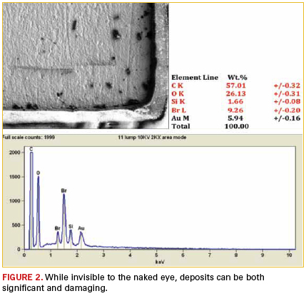
Undetected mask remnants can upset the final finish.
The arch-nemesis of final finish is solder mask. I am an expert in surface finishing. I understand the need for solder mask, but it is my right to dislike it. Truthfully, it makes my life more difficult, but those challenges help pay the bills. Solder mask brings out the ugliest in a surface finish, or so that is the perception. Research continues on how to build the widest operating window for a final finish, even when the problem falls outside the final finish line. I like to tell our development teams, “If research were easy, everyone would do it.”
Two main issues are associated with the solder mask process that later affect surface finishing: improper exposure and solder mask residues. Improper solder mask cure can affect the foot characteristics at the interface of the trace. If undercured, the solder mask will suffer chemical attack from the plating baths. This could result in one of two defects. Solder mask constituents leaching into the plating bath cause instability or plating-performance defects. Or, the chemical plating bath attacks the adhesion between the copper trace and solder mask. This creates a crevice for chemistry to become trapped. If overcured, solder mask can become brittle and fracture. Solder mask residues cause plating defects that may go undetected until the panel is post-assembly. Overall, improper solder mask application can wreak havoc on the final finish process.
The most infamous example of undercured solder mask effect on surface finishing was discovered in the early 1990s. Industry found a new post-assembly defect called “black pad.” Hot electroless nickel baths are the perfect environment to leach sulfur-bearing materials out of solder mask that has not properly cross-linked. This causes an increase of the “wrong” sulfur into the EN bath, which then co-deposits and alters the desired phosphorous content. The higher the sulfur in the EN deposit, the lower percent phosphorous included. Also, the type of sulfur included in the deposit can result in less corrosion resistance. This leaves a weakened nickel deposit that is more susceptible to corrosion in the electrolyte of the immersion gold bath. As the immersion gold bath corrodes the nickel, it leaves behind a phosphorous rich layer, which has poor solderability characteristics. The solder joints are weak, and the potential for components to pop off the PCB are greater. I still cannot resist saying, “Oh, there goes the BGA,” every time I drop my cellphone.
The second scenario observed when solder mask is undercured at the foot is a galvanic corrosion of the copper trace. This can be observed after immersion tin plating. All immersion tin baths contain thiourea; it is this material that drives the reaction. Without it, tin would not naturally plate on a copper surface. So the thiourea and acid in the immersion tin baths solubilize the areas of mask that are not cross-linked, leaving a negative foot. This crevice has a small geometry, which is difficult for solution exchange. Plating chemistry gets in and quickly depletes the metal, but then cannot get out for fresh replenishment of more metal. In essence, the solution trapped in the crevice has a high acid and thiourea content, which accelerates corrosion. As the uncured solder mask is removed from the foot and the copper trace corrodes, there is no longer an intimate connection between the mask and trace. This leaves a ledge of mask. Tape tests reveal solder mask adhesion issues around the pad edges at this interface. It is suggested to UV-bump panels prior to immersion tinning. This will help to cross-link any areas that did not go to completion in imaging. It should be noted that the darker the solder mask color, the harder they are to properly cure.
The most problematic defect coming out of imaging is residues on the pad surfaces. This is not cured solder mask; it is normally junk from the developer that redeposits on the board’s surface. The culprit is poor control or maintenance of the developer. Unfortunately, once the panels go through post-bake, these residues do cure and become extremely difficult to remove. The fun part is that solder mask residues are normally very difficult to see by eye, so they go unnoticed until after surface finish. Solder mask does not discriminate; it will prevent any non-HASL surface finish from coating properly. Depending on the degree of residues, it can go undetected even after the surface finish. But rest assured, it will cause a solderability problem.
So there are a few ways to address a solder mask residue issue. You can use a good cleaner designed to remove solder mask residues, but depending on the quality of the exposure, if the foot is soft, you will remove it and create the same crevice discussed above. Another option I really like is jet pumice. Unfortunately jet pumice gets a bad name, as it is associated with its cousin pumice (slurry) scrub. Pumice scrubbing utilizes a nylon brush that mechanically abrades the surface with the pumice slurry. The problem associated with this process is that the brushes can embed pumice into the copper. Once in, it’s not coming out. But jet pumice has no mechanical component; cleaning is driven solely by impingement, and it is a great tool for undermining solder mask residues on the copper surface.
As always, proper process control will lead to successful quality product. Don’t discriminate: There are multiple ways to create good product. Understand your options.
Lenora Toscano is final finish product manager at MacDermid (macdermid.com); This email address is being protected from spambots. You need JavaScript enabled to view it..