Hurricane Sandy poured rain on most contingency plan parades.
A funny thing happened on the way to – in fact just before – the recent US Presidential election. A mysterious lady showed up on the scene. Not necessarily a pretty one, but one bearing a larger than life persona who successfully took the mind of everyone within her wide swath off the election, or for that matter, everything else. That mysterious lady’s name was Sandy, and she again reminded those on the Atlantic Coast the US of what is really important.
And while those in other parts of the globe missed Sandy’s wrath, anyone who experienced the earthquake in Japan during 2011, the tsunami in Thailand that fall, or any of the typhoons that frequent the Southern Hemisphere understands the feeling of going to sleep one night with one plan only to wake up the next morning to a new world in which all notions of what’s important are turned upside down.
So what is important? Everyone would agree family and friends, health and safety. I would argue that relationships between customers and suppliers are important too. Possibly most important is the commitment to making sure that those within your scope of influence are protected from the misfortune and risk that natural and not-so-natural phenomena could cause.
Disasters have an uncanny ability to refocus us on the importance of contingency planning. Contingency planning is similar to other forms of “strategic” or “tactical” planning, except instead of considering desirable “what if” scenarios, it requires expending thought and effort on darker outcomes. Those dark outcomes include natural events (in insurance parlance, “acts of God”) such as fires, major storms, earthquakes, flooding, etc. But the dark side of “what if” also should include the consciously made “self-inflicted” decisions that sometimes just do not work out as planned and take a decidedly disastrous turn.
The easier, albeit not necessarily easy, contingency plans are those related to natural disasters. We all fear – and understand – the “what if” of a flood, storm or fire ravaging our facilities or their immediate surroundings, yet regrettably too few of us have an adequate contingency plan detailing how we would respond. For years, when asked what I would do if my plant burned down, I have jokingly replied, “File for Chapter 7.” But a simplistic approach is simply not the answer! There is so much more to consider: employees, customers, suppliers. The reality is that whether a major, game-ending event, or a minor one, a real plan needs to be thought through and ready for that “what if.” For those who do have a plan, should something happen to their individual facility, what if a disaster impacts more than just your site? What if a storm such as Sandy impacts a large region, or earthquake or tsunami devastates an entire country? How will your Plan B hold up in the case of such an event?
More difficult to plan for are those events caused by self-inflicted, poorly devised or executed decisions. Some could argue that a decision that could be as disastrous as even the worst storm is when management’s decisions exaggerate the natural workplace stress to the point of employee unrest or even suicides. Whether responding to a natural disaster or a manmade one, the outcome will be far worse without adequate contingency planning.
How do you plan for the unthinkable? Start by making a list of the stakeholders. Knowing who must be protected is a great first step toward planning protective actions. Safety and health come first, so the immediate catastrophe response most companies already have in place should be the foundation of any plan. Next is mapping a game plan that will assure customers and suppliers have a clear direction as to what you plan on doing, where and when. This planning is just as important as the safety of employees, as without customers and suppliers you might never reemerge from a disaster.
Next in the decision tree should be to map a plan for things you cannot control – external issues such as infrastructure destroyed to the point that even if your facility and employees come through unscathed, the ability to function is rendered impossible. This type of planning can only be done by conferring with local authorities so you understand their plans in the event of such a disaster. While never perfect, if minimally you end up at least knowing who to talk with in a given situation so you can determine the appropriate course of action in the case of an emergency, you will be far better off.
None of this is rocket science. The problem is, as simple as it may be, few of us actually have undertaken the effort to think through, communicate and document a contingency plan with the appropriate input from internal and local stakeholders.
And as few who have done any contingency planning for natural disasters, even fewer have thought through what to do if their decisions cause a life-threatening environment and/or disaster. Yes, individual conscience must dictate what types of events would be considered such a disaster; however, we should think through the typical decisions a company dealing with people, chemicals, equipment and deadlines makes and what to do if the outcome of those combined decisions has potentially life-threatening consequences.
So, while cruising along focused on an election, fate struck with a terrible storm and quickly refocused so many. We need to stay focused on making sure that when fate strikes, be it natural or self-inflicted, we have a well-thought-out contingency plan to help us through.
A look back at friends and colleagues who left us in 2012.
A pair of true industry giants died in this past year, both pioneers in their own right. Olin King founded Space Craft Inc., which under its more common name SCI Systems (and later, Sanmina-SCI), is generally recognized as the first contract electronics assembler and, for a time, was also the largest EMS company in the world. For his part, Gene Marsh was an electronics design automation pioneer, bolting Raytheon for a career developing PCB software for the masses. The Gene Marsh Award for Technical Innovation is named for him.
Two other major league inventors also passed this year. All couch potatoes owe a nap of gratitude to Eugene Polley, who over his 47 years at Zenith rose from stock boy to become assistant division chief of Mechanical Engineering and counted the first wireless remote control among his 18 US patents. And anyone who sees the promise of green energy can appreciate Stanford Ovshinsky, who was assigned more than 400 patents, the most significant of which – the NiMH battery – is used in everything from laptop PCs to cellphones to electric cars, and who later developed flat screen LCDs and thin-film solar cells. This month we reflect on their impact on our industry and our lives.
(Harold) Gene Marsh, 84, launched PADS Software in 1975, one of four companies he founded.
Olin King, 78, founder Space Craft Inc. (later, SCI Systems); credited with founding the modern contract electronics assembly industry.
Robert (Bob) Bukowsky, 71, former IDEAL vice president of sales.
James Lee, 51, founder of PCB fabricator UniGlobal.
Mr. Xie, age unkown, Foxconn employee.
Steve Appleton, 51, CEO of Micron Technologies.
Jackki Morris-Joyner, longtime IMAPS technical program manager.
Stanford R. Ovshinsky, 89, semiconductor expert who invented the nickel-metal hydride battery and codeveloped solar energy panels and flat-panel displays.
Robert (Bob) Parker, 53, computer engineer at Universal Time Co.
David B. Speer, 61, ITW chairman and CEO.
Chris Lewis, 64, president, CEO, and co-founder of Dynawave Inc.
Hans Camenzind, 78, analog guru who introduced the phase-locked loop to IC design.
Mr. Yang, 22, Foxconn Shenzhen.
Eugene Polley, 96, longtime Zenith Electronics engineer and inventor of the wireless television remote control.
And one in late December 2011:
Gene Hendrickson, 79, former Tektronix engineer, president of General Management Integration (GMI), and founder of the October Project.
It was a fairly quiet year for acquisitions. AsteelFlash, a former CIRCUITS ASSEMBLY EMS Company of the Year, and Creation Technologies, this year’s winner (see story, pg. 30) made their near-obligatory deals, but for the most part, the top two EMS tiers were quiet, while Viasystems’ purchase of DDi and Cadence’s acquisition of Sigrity, respectively, were the largest two fab and design deals. Then in early November, the earth was shaken by two huge announcements.
In early November, just days after Cookson announced it would split in two and spin out Alpha Metals and Enthone as a separate company, Dover said it too would divest its electronics assembly and test businesses. And just like that, we are primed to lose two of the longstanding electronics supply-chain brand owners.
For Cookson customers, the first question must be, what will this mean for Alpha and Enthone? My take is not much. Here’s why:
1. The company will remain public, and the shareholders are the same. (Under the proposal, Cookson shareholders get one share in each of the two new companies.) Had this been an MBO or private equity deal, I would expect slash and burn. But the transition as planned should bring much-desired stability to the new organization.
2. The upper management isn’t changing. Had Cookson Performance Materials group CEO Steve Corbett left, I might think differently. But Corbett, who joined Cookson in 1990 and has run Enthone since 2002 and both companies since 2004, is highly responsible for the existing management and operational structure. He knows what he is doing, knows the markets and understands the brands.
3. The debt is manageable. Alent (the new name of the former Cookson Performance Materials) will “get” about one-third of Cookson’s £451 million ($727 million) worth of debt. Given the new company’s sales of £418 million ($675 million) and profitability, it should be able to swallow that meatball.
4. The brands are intact. The Alpha and Enthone brands are well-recognized and respected worldwide. Indeed, after spending some time trying to beef up the somewhat unwieldy Cookson Performance Materials name, the company reversed gears and has been working over the past year to rebuild those individual brand names. Perhaps this was in anticipation of the demerger, but either way, the strategy was well-timed.
In fact, the only casualty I see in all this is the 300-year-old Cookson name. One wonders whether it was seen as a negative by either of the spinoff companies. And so goes Cookson. From its founding by Isaac Cookson in 1704 as a collection of metal and glass businesses to its aggregation and subsequent divestment of a herd of electronics equipment and materials companies in the 1980s and 1990s, Cookson has always been in a transition of some sort. This latest move appears to be its final one.
As we went to press, the future of the Dover businesses was much less clear. Dover hasn’t said whether it will sell the businesses piecemeal, as it did with Universal Instruments and Vitronics-Soltec in 2006. The brands on the block – DEK, OK International and Everett Charles Technologies among them – probably brought in at least $1 billion in annual revenue prior to 2012’s drop-off, and have traditionally been higher margin performers as well. Not many equipment companies have pockets deep enough to absorb the price Dover will ask. Yet that’s what employees of those businesses must be hoping for right now, as the scorched earth tactics of the private equity companies have been excruciating for everyone involved.
We don’t think this was a quick decision brought about by this year’s slump. Sources tell us Dover has been discussing the possible divestiture of these businesses for nearly a year. The guess here is that Dover’s management is tired of the endless boom-bust cycles of the electronics industry. It’s hard for an equipment company to meet Dover’s goal of 10% revenue growth and 15% operating margins year in, year out. We also believe Dover has a buyer on the hook, as some might recall that when Dover announced the impending divestiture of Universal, the deal went through a month later. Who that buyer is (ITW? Nordson?), and at what price, are now the questions.
Urgent ‘bulletin.’ In November, we launched Board Talk, the bulletin board for the PCB industry. The new board – theprintedcircuitboard.com – has categories for PCB design, fabrication, assembly, market data, trade shows and press releases. Members are invited to create their own topics (threads) for discussing anything industry related that they have on their mind.
We also are happy to announce an agreement with the IPC Designers Council to offer Board Talk as a communications center for news, announcements and meetings, plus information on the Designers Certification program. Please check it out.
“Process Development for Micro-Electronics Packaging with Direct Printed Additive Manufacturing”
Authors: R. X. Rodriguez, K. Church, Ph.D., and X. Chen; This email address is being protected from spambots. You need JavaScript enabled to view it.. Abstract: Using additive manufacturing as an alternative for packaging has not been taken seriously, but there is an opportunity to demonstrate the significant advantages of true 3D electronic packages by permitting the package to be the printed circuit board and by utilizing direct print and bare die approaches to print and structure diverse electronics. In order to build a device by implementing an additive, layering process, materials must be studied and characterized for repeatability and reliability of mechanical and electrical performance. This paper summarizes a study of some of the materials and the process used to build 3D structures using DPAM. Also described are variables that are adjusted to optimize a build with a DPAM process. A carbon nanotube – photopolymer composite, conductive ink, conductive adhesive and standalone photopolymer were tested for their individual electrical resistances, as well as the resistances when layered on each other. A single layer (~100µm thick) was dispensed then tested for its electrical resistance. The final build consists of three layers with a surface-mounted active component placed and electrically epoxied in place. (SMTA International, October 2012)
Component Packaging
“3D Packaging for High Computing with Wide IO Processor-Memory Interface”
Authors: Ilyas Mohammed, Ron Zhang and Rajesh Katkar; This email address is being protected from spambots. You need JavaScript enabled to view it.. Abstract: Current interconnect technologies for package-on-package such as stacking with smaller sized solder balls, using solder-filled laser-drilled vias in the mold cap, or using organic interposers are not practically achieving high IO requirements, since the aspect ratios of these interconnects are limited. To address the gap in PoP interconnect density, a wirebond-based package stacking interconnect technology called Bond Via Array is presented that enables reduced pitch and a higher number of interconnects in the PoP perimeter stacking arrangement. The main technological challenges are identified and research results explained. The main challenges were forming freestanding wirebonds, molding the package while exposing the tips of the wirebonds, cleaning the wire tips and package stacking. Assembly results showed that the wire tips were within the desired positional accuracy and height, and the packages were stacked without any loss of yield. (SMTA International, October 2012)
Semiconductor Fabrication
“High-Density Integration of Carbon Nanotubes via Chemical Self-Assembly”
Authors: Hongsik Park, et al; This email address is being protected from spambots. You need JavaScript enabled to view it.. Abstract: Carbon nanotubes have potential in the development of high-speed and power-efficient logic applications. However, for such technologies to be viable, a high density of semiconducting nanotubes must be placed at precise locations on a substrate. Here, the authors show that ion-exchange chemistry can be used to fabricate arrays of individually positioned carbon nanotubes with a density as high as 1 × 109 cm−2 – two orders of magnitude higher than previous reports. With this approach, the authors assembled a high density of carbon-nanotube transistors in a conventional semiconductor fabrication line and then electrically tested more than 10,000 devices in a single chip. The ability to characterize such large distributions of nanotube devices is crucial for analyzing transistor performance, yield and semiconducting nanotube purity. (Nature Nanotechnology, Oct. 28, 2012)
Solder Joint Reliability
“Impact of Electrical Current on the Long-Term Reliability of Fine-Pitch Ball Grid Array Packages with Sn-Ag-Cu Solder Interconnects”
Author: Tae-Kyu Lee, Ph.D. Abstract: The interaction between electrical current and long-term reliability of fine-pitch BGAs with Sn-3.0Ag-0.5Cu (wt.%) solder ball interconnects is investigated. In this study, 0.4mm fine-pitch packages with 300µm-diameter SnAgCu solder balls are used. Electrical current was applied under various conditions to two different package substrate surface finishes to compare the effects of chemically unmixed and mixed joint structures: a Cu/SAC305/Cu structure and a NiAu/SAC305/Cu structure, respectively. To study the thermal impact on thermal fatigue performance and long-term reliability, the samples were thermally cycled from 0° to 100°C with and without current stressing. Based on Weibull plots, characteristic lifetime was degraded for the mixed joint structure, but little degradation was observed for the unmixed joint structure. The microstructure evolution was observed during constant current stressing and current stressing during thermal cycling. Accelerated intermetallic precipitation depletion at the package-side interface was observed in NiAu/SAC305/Cu structures due to current stressing, which was identified as the potential reason for the degradation in the thermal cycling performance. (Journal of Electronic Materials, Oct. 28, 2012)
This column provides abstracts from recent industry conferences and company white papers. Our goal is to provide an added opportunity for readers to keep abreast of technology and business trends.
Written by Ephraim Suhir, Laurent BECHOU and Alain Bensoussan
Category: 2012 Articles
The state of reliability of the today’s complex and costly electronics and photonics systems should be checked (monitored) and, if possible and feasible, even managed on a continuous basis. This is particularly true for systems where failure-free operation is especially important. The objective of technical diagnostics (TD)1,2 is to recognize, in a continuous fashion and without taking apart the object of interest, its technical state and its ability to continue to perform in the expected (specified) fashion. TD establishes the links between the observed (detected) signals, the so-called “symptoms of faults” (SoF), and the underlying hidden state (“health”) of the device or the system of interest. TD effort is naturally focused on the most vulnerable elements (weakest links) of the design and can use the failure-oriented accelerated test (FOAT) data3 conducted in the design stage.
TD is an important part of reliability engineering and encompasses a broad spectrum of problems associated with obtaining, processing and assessment of diagnostic information, including diagnostic models, decision making rules and algorithms. TD provides information for the subsequent prognostics and health monitoring/management (PHM) effort.4 TD has to devise solutions and recommendations (“educated guesses”) under conditions of uncertainty and with limited information. Therefore the TD methods, techniques and algorithms are based, as a rule, on the probabilistic risk management and applied probability bodies of knowledge and are supposed to quantify, on the probabilistic basis, the obtained information (signals, SoF) and to provide assistance in making a decision if the device or a system of interest is still sound or has become faulty. There is always the possibility that the interpretation of the obtained SoF signal might be a false alarm or might lead to a missing-a-target decision. Statistical theory of decision-making, which is widely employed in radar engineering and is part of the TD, can be effectively used to avoid a false-alarm/missing-a-target mistake.
The objective of the analysis that follows is to show how the statistical Bayes formula (theorem) to update beliefs5-10 can be used to interpret the TD (PoF) information and to determine if the device (system) of interest is still sound (healthy) or has become faulty, and to use this information to identify a faulty device, if any. Then a reliability physics-oriented Boltzmann-Arrhenius-Zhurkov (BAZ) model11-13 can be employed to estimate the remaining useful lifetime (RUL)4,14 of a damaged (faulty) device. When the PDfR concept is used,2,15 such an assessment will lead, of course, to different RUL predictions, depending on the level of the allowable probability of failure (PoF).
Bayes formula in TD problems. Bayes’ theorem to update beliefs is widely used in many areas of applied science, engineering, economics, game theory, medicine and even law. In this section we interpret the Bayes’ formula in application to TD problems.
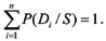
Let an event S be the observed (detected) signal (SoF), such as, e.g., measured elevated off-normal temperature, elevated leakage current, drop in the output light intensity, elevated amplitudes (power spectrum) of the induced vibrations, etc., and the events Di, i = 1,2,3...be possible malfunctions, diagnosed deviations from the normal operation conditions of the product (system) elements that might be responsible for the observed symptom(s). It is assumed that one and only one of the product elements is damaged to an extent that its detected off-normal performance has manifested itself in the observed symptom. Simultaneous failure (damage) of two or more systems’ elements is deemed to be extremely unlikely and is excluded from consideration.
Let one know the typical probabilities P(Di) of failure of its particular elements, based on the accumulated experience for the type of the device or system in question. The problem of interest can be formulated this way: The event (signal) S is observed for the given device (system) in operation. What is the probability that it is the system’s particular i-th element that has become faulty and is therefore responsible for the detected symptom?
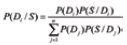
The Bayes formula
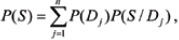
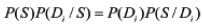
enables one to determine the posteriori probability P(Di)/S), after the symptom S has been detected, from the priori probability P(Di) of the typical, known from the previous experience, probability of the system’s state. The Bayes formula can be obtained from the complete probability formula
and the relationship
Formula 2 reflects a postulate that if a system has several possible and incompatible ways to get transferred from the state Dj to the state S, the probability of such an event can be found as the sum of the conditional probabilities of occurrence of each of these ways. Formula 3 indicates the probability of the simultaneous occurrence of the symptom S and the system condition (diagnosis) Di.
As follows from Bayes formula,
Bayes method is simple, easy-to-use and effective, and is widely used in many applied problems. Its shortcomings are the large volume of the required input information and “suppression” of seldom diagnoses.
Example 1. Let it be established from experience with the given devices or systems that 90% of the devices do not fail during the designated time of operation, and the symptom S, which is the increase in temperature by 20˚C above the normal level, is encountered in 5% of the cases (devices). The probabilities P(D1) and P(D2) of the sound condition D1 and the faulty condition D2, respectively, in the general population of devices are P(D1) = 0.9 and P(D2) = 0.1, respectively. The conditional probabilities are P(S / D1) = 0.05 and P(S / D2) = 0.95. Let us determine the probability that the device, in which the increase in temperature is detected, is sound. The Bayes formula yields
Thus, the probability that the device is still sound has decreased because of the detected increase in the observed temperature, from 0.90 to 0.32.
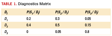
Example 2. The TD instrumentation has detected two deviations (SoF) from normal operation conditions: increase in temperature by 20˚C in the region of the heat sink location (symptom S1) and increase in the power of the vibration spectrum by 20% (symptom S2). It has been established that these symptoms might be due to the possible malfunction of one of the two pieces of hardware: heat sink (state D1) and/or vibration damping equipment (state D2). It has been established also that the symptom S1 (increase in temperature) is not observed at normal operation condition (state D3), and the symptom S2 is observed in 5% of cases (devices). Based on the existing experience of employing the devices of interest, it has been established that 80% of the devices do not fail during the specified time of operation; 5% of the devices are characterized by the state D1 (malfunction of the heat sink), and 15% are characterized by the state D2 (malfunction of the vibration damping system). It also has been established that the symptom S1 is encountered in the state D1 in 20% of the devices, and in the state D2 in 40% of the devices; that the symptom D2 is encountered in the state D1 in 30% of the devices, and in the state D2 in 50% of the devices. This information can be conveniently presented in the form of a diagnostic matrix (Table 1).
Let us determine first the probabilities of the device states, when both symptoms, S1 and S2, have been detected. The Bayes formula1 yields
Similarly, we find: P(D2 /S1S2) = 0.91; P(D3/S1S2) = 0. Determine now the probability of the device state, if the observations indicated that there was no increase in temperature (the symptom S1 does not take place), but the symptom S2 (increase in the power spectrum of the induced vibrations) was detected. The absence of the symptom S1 means that the symptom of the opposite event takes place, so that . Changing the probability P(S1/Di) in the diagnostics matrix to we find
Similarly, we obtain : Determine now the probabilities of the device states when none of the symptoms takes place. By analogy with the above calculations, we find
Similarly, we obtain: The calculations indicate that when both symptoms S1 and S2 are observed, the state D1 (the heat sink is malfunctioning) might occur with the probability 0.91. When none of these symptoms is observed, the normal state D3 is characterized by the probability 0.92 and is the most likely one to occur. When the symptom S1 (elevated temperature) is not observed, while the symptom S2 (elevated vibrations) is, the probabilities of the states D2 (damping system is not working properly) and D3 (both heat transfer and vibration damping hardware work normally) are 0.45 and 0.41, respectively. Since these probabilities are close, additional information based on observations and/or modeling might be needed to obtain more accurate diagnostics information.
Boltzmann-Arrhenius-Zhurkov’s (BAZ) model. Bayes formula (1) does not require any information about the physical nature of the obtained signals. When there is a reason to believe that the combination of elevated temperature and stress (not necessarily mechanical) can lead to a malfunction of a device or a system, the additional information about the possible source of the deviation of the system’s state from the normal operation conditions could be obtained by using Boltzmann-Arrhenius-Zhurkov (BAZ) model11-13
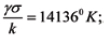
that enables one to evaluate the mean time to failure (MTTF) τ from the known applied stress σ (not necessarily mechanical); the absolute temperature Τ, the time constant τ0, the (stress-independent) binding (activation) energy U0; k = 1.3807 x 10⁻²³J/0K is Boltzmann’s constant, and the factor γ is the material (device) constant that is a measure of the vulnerability of the material to the applied stress and is measured by energy per unit stress, so that the product γσ measured in energy units.
BAZ model proceeds from the rationale that although the process of accumulation of damages is temperature dependent, it is influenced primarily by an external loading of any relevant nature. In other words, the model is based on the recognition of the experimentally observed situation that the breakage of the chemical bonds in a material under stress is due primarily to this stress, while temperature plays an important, but not a prevailing, role. Since the BAZ model contains three empirical parameters, activation energy U0, parameter γ of the level of the disorientation of the molecular structure of the material, and the time constant τ0, three failure-oriented accelerated test (FOAT) series should be conducted to determine these parameters.
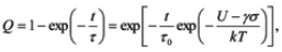
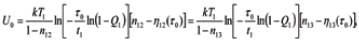
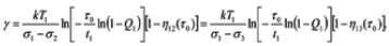
Let FOATs characterized by their absolute temperatures T1, T2 and T3 and applied stresses σ1, σ2 and σ3 be run until failures, and the respective measured times-to-failure (TTF) be t1, t2 and t3, respectively. Based on the observed percentages of failed devices, the probabilities of failure (PoF) where established are Q1, Q2 and Q3 respectively. Assuming that the BAZ model and the exponential law of reliability are applicable, the PoF can be defined as
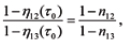
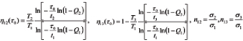
where t is time in operation. The time constant t0 in the BAZ model can be found from the transcendental equation
where the following notation is used:
Then (stress-free) activation energy U0 and the factor γ of loading (power) in the BAZ model can be computed as
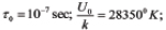
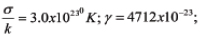
Example 3. Let, e.g., the FOAT carried out until half of the population fails (Q1 = Q2 = Q3 = 0.5) indicate that
so that then, for the operation temperature of T = 110˚C = 383˚K, the BAZ formula yields: years. The MTTF will decrease to
years. For the 20˚C increase in temperature, and will be only
days for the 20% increase in the power of the vibration spectrum. Although, as is evident from the obtained data, the faulty damping hardware could result in a significantly lower lifetime than the defected heat removing hardware; the damage in the damping hardware, based on the Bayes formula prediction, is much less likely than that in the heat sink.
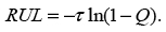
Example 4. Let us define the remaining useful lifetime (RUL) as the time between the moment when the diagnostic instrumentation has detected the malfunction (in the case in question it is the heat sink) and the moment of time when the PoF reached the allowable level Q. Assuming that the exponential law of reliability is valid (this law is characterized by the largest entropy and, hence, is the most conservative one), we find the RUL as
Assuming, e.g., Q = 10-3, we conclude that although the RUL is only years = 2.4070 days, this time is sufficient, however, to replace the faulty heat sink or the heat spreader or to fix the damage. If, however, the specified allowable level of the PoF is as low as Q = 10-5, the expected RUL becomes as short as
years = 34.6min.
There is not very much that could be done to restore the system’s reliability and to maintain it on the high level.
Conclusion
By combining the statistical Bayes formula and the physical BAZ model, one can obtain useful diagnostic information about the state of an electronic or photonic device or a system, subjected to the temperature-vibration bias. This information can be used as input data for the subsequent PHM effort. The suggested methodology is viewed as part of the general PDfR approach and can be used in the analysis, design and operational reliability assurance of electronic and photonic devices and systems, when reliability is imperative and its quantification is therefore a must.
References
1. H. Czilos, ed., “Handbook of Technical Diagnostics,” Springer, 2013. 2. E. Suhir, “Applied Probability for Engineers and Scientists,” McGraw-Hill, 1997. 3. E.Suhir, R.Mahajan, “Are Current Qualification Practices Adequate?” CIRCUITS ASSEMBLY, April 2011. 4. M.G. Pecht, “Prognostics and Health Management of Electronics,” John Wiley, 2008. 5. S.B. McGrayne, “The Theory That Would Not Die: How Bayes’ Rule Cracked The Enigma Code, Hunted Down Russian Submarines, & Emerged Triumphant from Two Centuries of Controversy,” New Haven: Yale University Press, 2011. 6. T. Bayes and R. Price, “An Essay Towards Solving a Problem in the Doctrine of Chance.” By the late Rev. Mr. Bayes, communicated by Mr. Price, in a letter to John Canton, M. A. and F. R. S. Philosophical Transactions of the Royal Society of London, 53 (0), 1763. 7. L. Daston, “Classical Probability in the Enlightenment”. Princeton Univ Press, 1988. 8. S.M. Stigler, “Who Discovered Bayes’ Theorem?” The American Statistician 37(4), 1983. 9. Edwards, A. W. F. (1986), “Is the Reference in Hartley (1749) to Bayesian Inference?” The American Statistician, 40(2), 1986. 10. S.E. Fienberg, “When Did Bayesian Inference Become ‘Bayesian?’ ” Bayesian Anal., Jan. 2006. 11. S. N. Zhurkov, “Kinetic Concept of the Strength of Solids,” Int. J. of Fracture Mechanics, vol. 1, no. 4, 1965. 12. E.Suhir, R. Mahajan, A.E. Lucero and L. Bechou, “Probabilistic Design-for-Reliability Concept and Novel Approach to Qualification Testing of Aerospace Electronic Products,” IEEE Aerospace Conference, March 2012. 13. E. Suhir, “Predicted Reliability of Aerospace Electronics: Application of Two Advanced Probabilistic Concepts,” IEEE Aerospace Conference, March 2013, to be presented and published. 14. E. Suhir, “Remaining Useful Lifetime (RUL): Probabilistic Predictive Model,” International Journal of PHM, vol. 2(2), 2011. 15. E. Suhir, “Probabilistic Design for Reliability,” Chip Scale Review, vol. 14, no. 6, 2010.
Ephraim Suhir, Ph.D., is Distinguished Member of Technical Staff (retired), Bell Laboratories’ Physical Sciences and Engineering Research Division, and is a professor with the University of California, Santa Cruz, University of Maryland, and ERS Co.; This email address is being protected from spambots. You need JavaScript enabled to view it.. Laurent Bechou, Ph.D., is a professor at the University of Bordeaux IMS Laboratory, Reliability Group. Alain Bensoussan is EEE senior parts engineer, Thales Alenia Space France.
From the US and Europe to Japan, cutting-edge technology is always on the move. Is it Taiwan’s turn to assume the mantle?
The technology arc in the interconnect manufacturing industry is once again in motion. Twenty years ago the United States and Western Europe were the sources of innovation in manufacturing processes.
New equipment and technologies were developed in cooperation with leading American and European fabricators such as IBM, Hewlett Packard and Cray Research. Independents such as Advanced Circuits for wireless and Photocircuits in automotive circuit boards led the way in developing new manufacturing processes. Today, all of those names are history in the interconnect manufacturing business.
The arc then shifted to Japan, where IC packaging substrates and high-density consumer electronics became the technology drivers. Designs for fine pitch rigid/flex, organic packages, and notebook computers drove high density interconnect with a wave of specialty technologies. Embedded components began to be used in consumer products. Japanese companies are still driving much of the technology, but are doing it in an accelerating manner offshore.
Today, Taiwan is set to take the torch. The first tier Taiwanese PCB manufacturers are now in discussions with key customers on pushing closer to 10µm lines and spaces for interconnect substrates containing active components. Shorter signal paths, profile reduction, and product security all play a factor in this drive. If you were to ask an American or European fabricator to build such product, they would look at you like a Martian. In Taiwan with ready capital, government support, and an already outstanding technology base, they would ask, “How many sets?”
The distance between Taoyuan County, where much of the interconnect industry is located, and the Hsinchu Science Park, where much of the R&D and Taiwan’s formidable semiconductor industry resides, is less than 70 miles. This does wonders for technology development.
But the greatest drivers are still external. It is the North American OEMs driving the technology, and the leading European, American, and Japanese suppliers who are at the fore in materials, process and technology. But it is Taiwanese companies synthesizing these ingredients into the next generation of technology.
Business conditions. Businessmen talk. Information is a commodity, and the first question after catching up is usually “how’s business?”
From reports all over Asia, business is very soft. The top tier interconnect manufacturers are off by 15 to 20%, while many others are down by 25 to 30%. A few, especially commodity manufacturers in China, are down as much as 40%. International materials suppliers are down 15 to 20%, and few are holding their own simply by partnering with the right circles. Small hole drill bit usage in Asia is down 25%, while solder mask usage is down as much as 30%.
Several new plants are being designed and built, including a very large project at KCE. AT&S’ new HDI plant in Chongquing is just about to come on line, while Ibiden is expanding in Malaysia. There is a strong trend of Japanese manufacturers moving new production away from China because of the current political environment.
The tension between China and Japan is also affecting current business. There have been reports of Japanese components, machinery and materials mysteriously tied up in customs, which is now affecting production and deliveries to end-users. This could be a double-edged sword if this trend continues and factories are forced to slow or stop production because of shortages.
There is the Apple Circle, the Samsung Circle and the Intel Circle. If you know the secret handshake, your company is doing okay, but even then there is the risk of allowing too much of one’s capacity to be driven by a few customers. Forecasts for 2013 are more positive, but there is a long way yet to go. The European economic slowdown and uncertain demand in North America are also impacting the industry, while weak automotive sales in China and consumer conservatism in that market have not been able to take up excess capacity.
Technology improvements. The most striking news in the technology of the interconnect was sub-10µm lines and spaces.
A very few companies have been manufacturing limited quantities of 15µm line/space product, primarily for packaging applications, but now there is a roadmap including both 10µm geometries and embedded actives.
This will be another phase shift in the materials and equipment of interconnect manufacturing, as the requirements approach those of what was in the semiconductor field 30 years ago. A number of imaging equipment manufacturers have been developing or delivering stepper systems, while wet process suppliers have been inching toward these demands as well. Completely new processes will have to be developed, and it is likely that process chemistry will also require ultra-pure formulations to prevent contamination.
The influence of 3D IC packaging on the interconnect was also a major topic of discussion. Chip-scale packaging is going mainstream, and all of the factors of substrate stability, 35µm pitch, and how to process organic substrates for 3D applications are at the top of the list. TSMC and other fabs will begin production in the first quarter 2013, so the issues are real and immediate. Design tools for 3D IC substrates are in place, and several interconnect manufacturers have established dedicated production lines, but the next year will be one of challenges as volumes rise.
Thermal, mechanical and electrical integrity are more important than ever, as stacked chips present challenges to the interposer. This then goes back to integrating passive devices within the package as well, and the issue of known good die becomes critical. The interconnect is becoming the device. 3D IC is also shaking up the OEM world. Fabless semiconductor companies are finding themselves at a distinct disadvantage, and a number of business models have been changing. Suddenly, major corporations such as Qualcomm, Broadcom and AMD are more vulnerable and constricted in their ability to move rapidly with new designs.
There were fewer Westerners than ever at this year’s TPCA, and yet to understand the means of production, this is one of the best venues in the world. If we do not understand how the product is built, we cannot build the next generation. There has been a move toward reshoring, or returning production to North America and Europe. The reasons range from a less competitive China to quality to being closer to end-users. But if the infrastructure does not exist for a critical technology such as the interconnect, what happens?
A final note. John Mitchell, the new president of IPC, was everywhere at TPCA, meeting with as wide a range of stakeholders as possible. He is a listener and a doer and has already had a very positive impact on the direction of the organization. In times when the challenges are great, it takes cooperation and collaboration to make significant progress. It is good to see that the suggestions of stakeholders are being considered and addressed and to see real world results.
Matthew Holzmann is president of CGI Americas (cig-americas.com); This email address is being protected from spambots. You need JavaScript enabled to view it..


 of the opposite event takes place, so that
 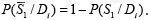 . Changing the probability P(S1/Di) in the diagnostics matrix to
  we find
 : Determine now the probabilities of the device states when none of the symptoms takes place. By analogy with the above calculations, we find
 The calculations indicate that when both symptoms S1 and S2 are observed, the state D1 (the heat sink is malfunctioning) might occur with the probability 0.91. When none of these symptoms is observed, the normal state D3 is characterized by the probability 0.92 and is the most likely one to occur. When the symptom S1 (elevated temperature) is not observed, while the symptom S2 (elevated vibrations) is, the probabilities of the states D2 (damping system is not working properly) and D3 (both heat transfer and vibration damping hardware work normally) are 0.45 and 0.41, respectively. Since these probabilities are close, additional information based on observations and/or modeling might be needed to obtain more accurate diagnostics information.
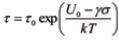
 then, for the operation temperature of T = 110˚C = 383˚K, the BAZ formula yields:


 years = 2.4070 days,
  years = 34.6min.

