Open source designs are becoming widely – and freely – available.
Multiple CAD and CAM companies’ tools from Altium to Ucamco to Cadence are now available via the cloud, albeit often through third parties. There is, however, one company that is a dedicated cloud-based CAD provider: Upverter. The company, which was founded less than two years ago, aims to leverage online collaborative tools to perform printed circuit design using a web browser and, in doing so, drive what they call the first real technology transformation since Windows.
Upverter (upverter.com) relies on nothing more than the user’s preferred browser. (Upverter says it supports 17 different browsers on a regular basis, although old versions of Internet Explorer aren’t among them.) Because the primary browsers interoperate, teams can work on their designs without necessarily adopting an identical platform.
Brower-based design tools aren’t easy to build, of course, but using them is another story, the founders say. Among the advantages are free access to extraordinary technology, no need for in-house servers, no real maintenance or IT. Or, as cofounder and CEO Zak Homuth says, “You remove a bunch of complexity and get a lot of stuff for free.”
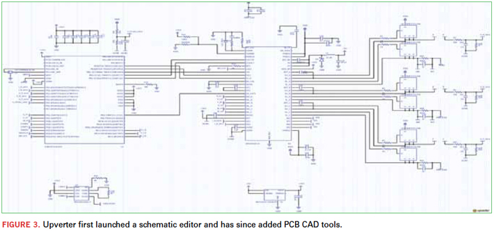
Upverter’s first product, which launched about 18 months ago, was a collaborative schematic editor. In November, they followed up with a major release that provides simulation, rapid prototyping, and involved a significant revamp to the schematic editor. At that time, the firm also released a new parts library.
And as it turns out, certain users, to date mostly hobbyists, can share in all that free stuff.
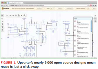
The firm has four basic pay models. The lowest price – free – comes with the limitation that all the designs, parts created or any other related IP are considered open source and available for public reuse. Upverter’s payoff is becoming notable: It boasts 8,000 to 9,000 available designs.
For those individuals who want some degree of privacy, the charge is a nominal $100 a year.
Team-based designers make up what Homuth calls the first “forced collaborative bucket.” This group pays about $100 a month for each user. Under this schedule, there’s no cap on the number of fulltime users, and designs can be sent to users outside the designated team who pay “by the hour” flex fees. There are no contracts, and fulltime users can be added or removed on a monthly basis.
The fourth level is the private cloud, designed for large corporations with perhaps thousands of users around the world. As Homuth describes it, this level offers higher level security, as the designs are not stored in the same place. Upverter also customizes the tools for this group.
“We’ve attempted to be able to charge the whole spectrum of people around the world and provide the services they need, but without limiting them as to what they can use,” explains Homuth. “There are guys in the basement who design motherboards. But teams by definition need collaboration.” As of late December, Upverter was approaching 10,000 users.
What those users are tuning in for is becoming more extensive. As Upverter’s first tool, the schematic editor is reasonably full featured, Homuth says. “We’re adding groups of nets and can display as a bus instead of as individual nets. We’re adding hierarchy modules (blocks) for designing a schematic within a schematic.”
Layouts have no limits: Designers can build an infinite number of layers. The tools can perform BGA breakouts, and differential pair and bus routing are being added. Much of these capabilities are a bit raw, Homuth admits, but are rapidly developing to full scale. Stackup and layer management features are available, but controlled impedance is not. “We are working with the Open Compute Project to get their server designs into Upverter to route DDR memory buses and control stackup, add prepregs, and do trace length matching of the whole bus. Those three features are really layout features and are on the cusp of being available,” he adds. Upverter lacks an autorouter at this time.
“The best way to describe our CAD is it’s like a machete: You can use it to do anything – you can use it to spread peanut butter or to cut down a tree. But it’s better for some things than others right now,” Homuth says.
The parts library contains 17,000 parts, all crowd-sourced and engineered by a user and subsequently edited by someone who wasn’t the creator. All users are notified of part updates, and have the option of accepting the update.
Users can export Gerbers, BoMs, and even an entire design as an open source file format using JSON (json.org). Another open source tool under development (https://github.com/upverter/schematic-file-converter) can convert any data into the CAD format of the user’s choice.
Much of the site’s appeal is the extensive IP available for reuse. There, Homuth says, one could find designs ranging from Arduino, Raspberry Pi and Internet of Things to distributed computing and sensor arrays. Shortly, all of SparkFun’s reference blocks will be available as well, and this month a few larger computer type designs will come online. These aren’t simply two layer boards with a handful of resistors. The average available design has hundreds of parts and maybe thousands of nets.
Security is handled the same as for anything stored in the cloud for credit cards or other personal information. Because the design never actually resides on the user’s PC, even an infected machine won’t comprise the data. “It’s just a jumble of data inside your web browser, and there’s a very good chance someone couldn’t reconstruct that even if they wanted to,” explains Homuth. “My anticipation is (hackers) wouldn’t know what they were looking at, and wouldn’t care.”
As any user knows, Java script can occasionally get in the way of browsers functioning properly. Upverter’s solution is to build on top of the same Google Java script program used for Gmail. That way, maintenance is Google’s problem.
Still, when Mozilla changed the way it implemented Canvas, the HTML element that can be used to draw graphics using scripting, Upverter quickly notified users of the affected version of Firefox about the glitch.
Asked how Upverter could keep its users up and running when it is reliant on third parties that might not share the CAD firm’s concerns, Homuth says it’s as simple as staying current on updates. “Because we are managing the data and compliance and migration, we are always up on the latest updates. You will never have the problem of an update conflicting with an old program. In exchange, you maybe have to update your web browser, but it’s a much more approachable problem for an engineer whose job is not maintaining IT systems and instead is designing PCBs.” For new designers or even veterans who don’t want to invest large sums in software, Upverter’s cloud-based CAD offers an airy solution.
[Ed.: To enlarge the figure, right-click on it, then click View Image, then left-click on the figure.)
Mike Buetow is editor in chief of PCD&F (pcdandf.com); This email address is being protected from spambots. You need JavaScript enabled to view it..
A look at a number of variables reveals certain implications for materials used as moisture barriers for components.
Moisture vapor and oxygen transmission are both important considerations for many polymer applications, including sensitive electronics such as semiconductors and display components. The requirements for barriers range from extremely high to moderately permeable. Moisture vapor transmission rate (MVTR) is described as the rate of gaseous H2O passing through a film or container. Oxygen transmission rate, or OTR, is the rate of oxygen passing through a film or container. The standard measurements for both properties are similar. MVTR is measured in grams of H20/m2/day (gH20/m2∙day), and OTR is measured in cubic centimeters/meter2/day (cc/m2∙day). Both barrier transmission rates can be expressed based on the thickness of the film or container. This property is called permeation. As an example, 1 mil of a standard PET film will have an MVTR of roughly 25 grams of H2O passing through 1 m2 of PET in one day (25 gH2O/m2∙day). Because the transmission rate is inversely proportional to the thickness, 5 mils of PET will have an MVTR of 5 gH2O/m2∙day. A 1 mil thick film of PET will allow approximately 6 cc/m2∙day of oxygen. And a 5 mil thick PET film will allow 1.2 cc/m2∙day of oxygen to pass. In the English system of measurements, the permeability is defined at a thickness of 1 mil; therefore, the moisture vapor and oxygen permeability of PET would be 25 (gH2O ∙mil)/(m2∙day) and 6 (cc∙mil)/(m2∙day), respectively. By knowing the permeability of a material, the MVTR and OTR can be calculated at any thickness.
Different methods of measuring and reporting permeation can cause confusion. Relative humidity, temperature and dimensions of the test protocol can create large differences in the reported permeation values. For example, while PET may typically exhibit 25 (gH2O∙mil)/(m2∙day) at 37.8°C and 100% RH, this number drastically decreases at lower humidity levels and temperature. The same principles are considered when measuring OTR; most testing procedures use 23°C and 0% RH. However, some procedures require humidity or temperature alteration that will drastically change the MVTR and OTR. In addition, some industries may report permeability per cm2, or by 1mm thickness, or other variations. This PET could have a permeability of 6.35E10-5 if the value is reported in (gH2O∙mm)/(cm2∙day), and even lower at 90%RH and 25°C.
Moisture vapor transmission rate and permeability are important parameters for some polymer applications, and understanding how the values are reported is also important. The results shown eliminate the variable of thickness by reporting permeability for MVTR in g∙mil/m2∙day at 100% RH and 37.8°C (100°F). For OTR, data are reported in cc∙mil/m2∙day at 0% RH and 23°C.
Experimental
Sample preparation. Different neat oligomers and several blends were examined for MVTR, OTR and permeability. Each UV curable resin or blend was mixed with 4% photoinitiator (KTO46) and cured approximately 7 (±2) mils thick on polished aluminum, using two passes at 50 fpm under two mercury arc lamps (400W/in) in air. The samples were then removed from the aluminum and cut into the appropriate size for moisture vapor and oxygen transmission testing.
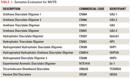
MVTR. The apparatus used for moisture vapor transmission testing was a Permatran W 3/33 from MOCON. The instrument parameters were 100% relative humidity, 37.8°C (100°F), and dry nitrogen flow rate of 100 sccm (standard cubic centimeters per minute). Samples were tested in duplicate and the average values taken for the result. The different samples were chosen to illustrate differences in permeability as a function of backbone chemistry, molecular weight, diluents of monomer, and crosslink density. A summary of the materials tested is shown in Table 1.
Samples were conditioned on the MOCON apparatus until equilibrium was achieved, typically for 12 to 24 hr. Equilibrium was defined as consistent results over a minimum 3 hr. time frame.
OTR. Many combinations of acrylate monomers and oligomers were sent to a third party to be tested for OTR. Samples were tested at 0% RH and 23°C. Oligomers and monomers ranging in functionality, aromatic/aliphatic urethane and epoxy backbones, and acid functional acrylates were all tested.
Calculations. Solubility parameters were calculated using the Hoy group contribution method, and were based on the idealized structure of the synthesized molecules. Unfortunately these are only calculations, and real experimental values would be more accurate for solubility parameters. Nonetheless, the author felt that these calculations provided some important insights into the nature of these results, so they were included.
Results and Discussion
MVTR. Several structural and chemical parameters had a notable influence on the moisture vapor permeability performance of the UV curable resins tested. The four primary factors contributing to the barrier performance of UV-cured polymers were 1) hydrophobic/hydrophilic nature, 2) molecular weight and crosslink density, 3) aromatic or cycloaliphatic nature, and 4) presence of unreactive fillers (solid particles).
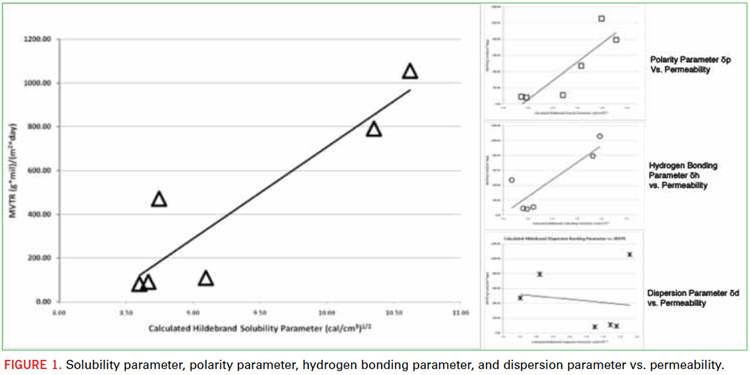
The first influence readily identified as a major influence on permeability is hydrophobic/hydrophilic nature. CN307, CN308, CN309, CN310, CN9014 and CN301 are all on the extremely hydrophobic end of the scale for UV/EB curable oligomers. Materials like CN964, CN966J75, and CN971 are also hydrophobic in nature but much less so than the aforementioned structures. Without any regard to the other identified contributors, Figure 1 depicts hydrophobic nature (calculated Hildebrand Solubility parameters [δ]) vs. permeability for the oligomeric structures tested for this work. It is also interesting to note that some components of the Hildebrand parameter, in particular polarity (δp) and hydrogen bonding (δh), have more influence over water vapor transmission rates than dispersion (δd).
[Ed.: To enlarge the figure, right-click on it, then click View Image, then left-click on the figure.)
Clearly the implication is that more hydrophobic materials provide a better barrier to the ingress of water vapor. This is as expected, and the correlation to the calculated Hildebrand values serves to identify these calculations as a potential screening tool in the design of new or untested resins and commercial products. For the majority of materials tested in these experiments, degree of hydrophobicity was the dominant factor in barrier performance.
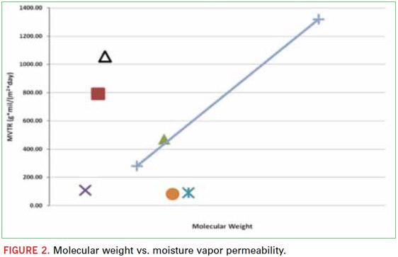
The second major influence on moisture barrier performance was molecular weight and crosslink density (Figure 2). Two oligomeric diacrylates with the same backbone chemistry, but different molecular weights, were tested. The lower molecular weight material exhibited much better barrier properties than the higher molecular weight oligomer. Backbone chemistry and the related degree of hydrophobicity had a much larger effect on barrier performance, but within the same backbone chemistry, lower molecular weight that yields shorter distance between acrylate-acrylate bonding exhibited barrier improvement.
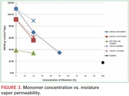
An easier way to evaluate the effect of crosslink density is to add varying concentrations of a low molecular weight diacrylate to increase crosslink density. In this experiment, hexanediol diacrylate (HDDA) was added at 20% by weight to some of the oligomers to observe this effect. Figure 3 shows that in all cases, the permeability decreased with the presence of HDDA, indicating that higher crosslink density and a tighter cured network improves barrier performance. In addition to HDDA, another monomer, tricyclodecane dimethanol diacrylate (TCDMDA) was added for comparison. The presence of TCDMDA, like HDDA, increased the crosslink density of the cured polymer and boosted the barrier performance. Both TCDMDA and HDDA are hydrophobic, but to a much lesser degree than the extremely hydrophobic oligomers; therefore, this effect can be attributed more to crosslink density and tighter network formation than to backbone chemistry and hydrophobicity.
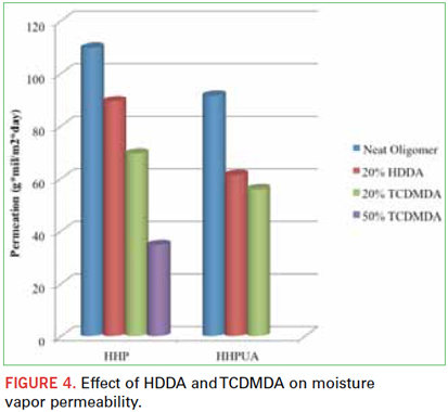
The next major contributor studied was the presence of aromatic and cycloaliphatic components in the cured polymer. It was shown that these two backbone chemistries improve barrier properties of similarly structured materials. A good example of this is the influence of HDDA vs. TCDMDA depicted in Figure 4. As discussed, lower molecular weight materials typically reduce permeability more effectively than higher molecular weight, but in this comparison, TCDMDA has a greater efficacy than HDDA, despite higher molecular weight (305 Daltons vs. 226 Daltons). Also interesting to note is that the number of carbons between acrylate groups for TCDMDA vs. HDDA is similar (7 vs. 6, respectively); therefore, the actual crosslink density is more similar than the molecular weight would suggest. Apparently the cycloaliphatic and more bulky backbone of TCDMDA better prevents ingress of H2O. At this point it should be noted that TCDMDA alone exhibited the best barrier performance: 17.8 (g∙mil)/(m2∙day) of any material tested in this experiment. Most likely this is due to the high crosslink density of the low molecular weight difunctional monomer and the overwhelmingly cycloaliphatic nature of its backbone. Aromatic backbones have a similar effect. A low molecular weight experimental product containing aromatic groups, NTX7418, exhibited low moisture vapor permeability of 69.5 (g∙mil)/(m2∙day).
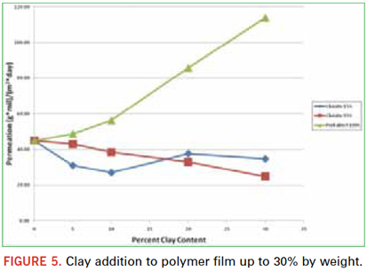
The presence of unreactive fillers can influence the barrier properties of UV/EB cured polymers. Several clay materials were tested at different concentrations. In Figure 5, it was observed that, depending on type and concentration, unreactive fillers can be effective at reducing the moisture vapor permeability. Other more effective fillers certainly can be used, but this is outside the scope of this work. An entire paper devoted to the study of various fillers and loadings could easily be justified. Here, three different clay products were tested at 5%, 10%, 20%, and 30% loadings by weight. It should be noted that there was a dramatic effect on viscosity at 20% and 30% loadings. As viscosity becomes higher, free films are more difficult to cast without any imperfections that may adversely affect barrier performance.
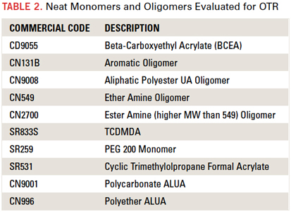
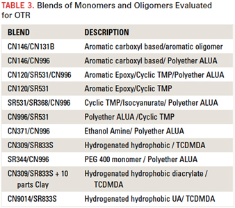
OTR. Many different monomer and oligomer structures were tested for OTR, but only a couple notable trends were observed. The samples displayed in Table 2 were neat monomers or oligomers prepared with 4% Esacure KTO46 photoinitiator and tested for OTR. In Table 3, blends of monomers and oligomers were evaluated using the same 4% photoinitator.
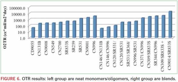
Figure 6 displays the oxygen permeation of both the neat and blended polymer films. It is evident that the hydrophobic/hydrophilic chemistries that lowered MVTR actually increased OTR. The CN309 and CN9014 blends are clearly much higher OTR than more polar molecules like CN146 and BCEA (Beta-carboxyethylacrylate). The low OTR is related to the concentration of carboxyl groups in the chemistry backbone. CN146 and BCEA contain carboxyl groups and yield a lower OTR permeation value. The negative polarity of the carboxyl groups helps to block negatively charged O2 molecules from passing through the polymer film. An ideal polymer-based oxygen barrier film would contain a tight network of polar molecules with a maximized concentration of valence electrons. Neat BCEA has the lowest oxygen permeation due to the higher concentration of electron’s in the polymer network.
Aromatic and highly polar molecules will create a greater oxygen barrier due to their electron densities or presence of electrons. In Figure 6, an aromatic ring structure, CN146, is added to an aliphatic urethane acrylate (ALUA) CN996, and a significant reduction in oxygen permeation is observed. This is due to both the higher concentration of carboxyl groups and the aromatic backbone of CN146. Additionally, CN120 is a bisphenol A-based acrylate, containing aromatic rings in the backbone, and it also significantly reduces the oxygen ingress of CN996. When an aliphatic monomer SR344 is added to the same ALUA oligomer, there is only a slight reduction of oxygen permeation compared to the neat ALUA oligomer. It is evident that with higher electron density backbone components, for example aromatic rings and carboxyl groups, a moderately high oxygen barrier can be created using UV/EB cured monomers and oligomers.
An additional observation is that unreactive fillers, such as clay, may have a negative effect on oxygen resistance. With the addition of 10 parts clay added to a formulation, an increase of 1,430 cc∙mil/m2∙day was observed. This is a result of the reduction of polar forces or opening non-polar pores in the polymer film that allows greater ingress of oxygen. Other types of polar fillers, such as silica or metal, could be considered for future study. Conclusion
The evaluation of the permeability of UV/EB cured polymers has highlighted several factors that influence performance. For MVTR, hydrophobicity, high crosslink density, and rich aromatic/cycloaliphatic content seem to be contributing factors for superior barrier performance. In addition, the use of unreactive fillers can provide an MVTR performance boost and an OTR drop. Although, this is not universal, and the types and concentration of fillers have not been exhaustively researched.
The results for OTR showed that it is important to use highly crosslinked aromatic and polar molecules to form a tight polymer network. A more concentrated grouping of highly polar and aromatic molecules will yield a better polymer oxygen barrier. For moderate to lower oxygen barrier properties, UV/EB cured polymer films are a viable option. For more demanding oxygen barriers, it is common practice to use polyvinylidene chloride (PVdc), polyvinyl alcohol (PVOH), or metallization layers. In the future of this study, it would be interesting to test fluroacrylate products for oxygen barriers, as other halogenated molecules demonstrate success. Other aspects of the polymers listed need to be addressed. The best performing MVTR polymer in this study, TCDMDA, does not have all of the ideal polymeric behaviors that are needed for every application. TCDMDA is very brittle and hard, with a high tensile strength and Tg. While this could be ideal for some applications, for flexible packaging for example, the properties are not ideal. Due to the high crosslink density of TCDMDA, shrinkage amounts can be high, and coatings thicker than 3 to 5 mils may crack simply from the polymerization/curing reaction. Similarly, even though BCEA exhibits good oxygen permeability, because of the acid functionality, it would not be suitable for moisture exposure.
Joshua M. Oliver is manager of UV specialty applications, and Dale S. Babcock is applications chemist at Sartomer (sartomer.com); This email address is being protected from spambots. You need JavaScript enabled to view it..
Working designs depend on understanding signal integrity, materials and plating.
High-speed backplane systems consisting of a printed circuit board (PCB) and interconnects maximizing signal integrity are the transmission paths providing financial services, military intelligence, commercial communication, and digital video links. Successfully introducing such a system requires technical expertise in PCB fabrication, experience with low-loss laminate materials, an understanding of signal integrity design, and knowledge of connector selection and application.
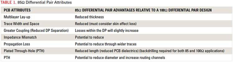
The connector influences backplane PCB design. Some come in ranges as high as 6.25 to 25Gb/s and employ differential pairs. The DP impedance choices often include 85Ω and 100Ω. The impedance selection depends on the semiconductor operating system. Table 1 depicts 85Ω differential pair attributes compared to 100Ω differential pairs.
[Ed.: To enlarge the table, right-click on it, then click View Image, then left-click on the table.)
During high-speed signal propagation, the signal predominantly travels along the conductor surface. A conductor’s surface roughness contributes to signal degradation. The total signal loss is the combination of the losses by the conductor and dielectric laminate. Since laminate or dielectric loss increases proportional with an increasing frequency, and the conductor loss is proportional to square root of the frequency, trace surface texture and width exhibits a smaller contribution to signal degradation. An 85Ω design having reduced trace width and laminate thickness, favorable electrodeposition within a plated through-hole, the potential to employ small diameter PTHs, acceptable production yields, and lower board fabrication complexity offers conceivable cost savings and improved fabrication predictability.
High-speed connectors often have finished PTH nominal diameters ranging from 0.46 to 0.60mm and, in accordance with RoHS, will have PTH finishes other than SnPb. These finishes may include immersion tin or electroless NiAu and require PTH tolerances often more stringent than those associated with SnPb finishes. Successful electrodeposition within these PTH holes depends on the fabricator’s technical expertise and is gated by the multilayer nominal thickness ratio to the finished PTH diameter. Reduced PCB thickness contributes to minimizing this ratio and promotes uniform metallization of the PTH wall and robust connection to innerlayer traces. Figure 1 depicts uniform PTH geometry and innerlayer connections.
Laminate material intrinsic properties, dissipation factor or loss tangent, Df and dielectric constant, Dk, PCB process stability, and transmission clarity define the end-product performance and predictable conformance to requirements. A technically competent backplane supplier has a relationship with the PCB supplier who has characterized the signal integrity variables, including the effective dielectric constant, Dkeff. The Dkeff accounts for the influence of the combined core and B-stage laminate upon impedance and signal propagation. There should be demonstrable process capabilities supporting composite construction, sequential lamination, back-drilling, and finishes providing RoHS compliance and long-term reliability.
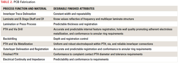
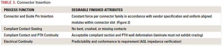
Having selected a prototype and production supplier that has foregone technical capabilities, comprehensive process predictability, conformance to requirements and consistency must be demonstrated through effective monitoring and statistical process control. This includes the fabrication process, assembly process, and the finished product’s electrical and mechanical performance. These process and finished product attributes have been tabulated in Tables 2and 3.
Many of the process functions shown in Tables 2 and 3 may be continuously monitored and predictability verified through the application of SPC, specifically control charts depicting upper and lower limits that conform to the unpopulated and populated backplane’s physical and electrical requirements. In addition to control charts, the process capability index should be known. Several companies have developed automated finished production monitoring test equipment applicable to the unpopulated and populated backplanes. Capabilities include measurements defining impedance, propagation delay, effective dielectric constant, S parameters, and verification of compliant contact seating.
When selecting a backplane manufacturing source, be it for prototypes, production or both, the following criteria summarize the material and technical function and backplane verification promoting efficient transition from design to viable hardware:
Demonstrated SPC, including incoming material, fabrication and electrical test, continuity and impedance.
Competent process control through the assembly operation employing control.
Charts reflective of compliant insertion parameters, x-ray verification and assembled electrical test.
Populated backplane electrical test beyond continuity to include impedance and S parameters. AQL may be applied to impedance and S parameter verification.
High-speed backplane fabrication and assembly meeting technical, price, and delivery requirements is readily achievable when a connector system is selected through knowledge of PCB fabrication and a thorough understanding of the required performance attributes and their applicability to system performance. Stringent and comprehensive quality control procedures drive cost efficiencies, on-time delivery, and consistent performance solutions.
Carl Hornig, P.E., is a consulting engineer and former technical director backplane fabrication, signal integrity, and assembly at Sanmina (sanmina.com); This email address is being protected from spambots. You need JavaScript enabled to view it..
It was almost forty years ago when I got my first job as a freshman in Japan, and to celebrate my “success,” I bought a high-end watch made by Seiko –a large watch manufacturer in Japan.
When should machine soldering be used instead of manual?
High-mix production is the mainstay of many electronics assembly plants. Lot sizes and board complexities vary, and boards are often mixed technology, comprising a blend of both surface-mount and through-hole technology. Modularizing a production line enables a clear distinction between one type of assembly process and another. This month, we look at the decision-making of routing a circuit board through-hand assembly vs. automated selective soldering. This assumes a modern factory where a job can be routed to the selective soldering machine module, the hand assembly bench, or a combination.
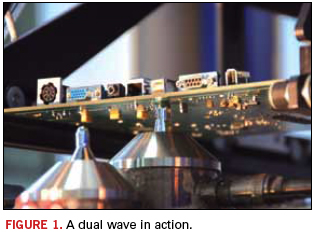
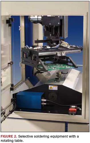
Selective soldering machines are an automated way to solder through-hole components on a circuit board. The machine contains a heated solder tank that generates a small fountain of molten solder approximately 0.375" in height and 0.25" in diameter. The leads to be soldered are positioned into this fountain of molten liquid for soldering (Figure 1) using a programmable x-y translation table. The operator places the PCB into the motorized x-y table (Figure 2) and by using a program (either input by the operator or imported from circuit board drawings), directs the board to move above the solder jet, lower a specific component into the solder fountain for soldering, raise the board, and translate the board to the next component to be soldered.
Modularizing the production plant enables the manager to match the production rate and precision requirements of a specific job with the correct machine or machine operation. A clear example of this modular approach is a comparison between routing a job between a hand-soldering operation and a selective soldering machine. Some decisions are obvious. After programming and setup of a selective solder machine, the process operation will always yield the same quality solder joint, repeatably. Hand soldering results can vary depending on the operator. This variation can be minimized if the assemblers are all trained to an industry standard like J-STD-001, Requirements for Soldered Electrical and Electronic Assemblies. This standard must be applied to the finished assembly, regardless of method of assembly, manual or automated.
Although surface mount is the dominant form of component today, some components may only be available in a through-hole format (such as power transistors and connectors). When a modular production line is set up, the decision of routing the job through the selective soldering machine may be based on the number of solder joints. If there are dozens to hundreds of joints to be soldered, the selective soldering path is a superior choice over a manual bench operation. If there are only a few joints to be soldered, hand assembly is a good choice.
Whether using manual or selective soldering, the board must be inspected by a human operator. This can reduce the efficiency of the automated process. With this in mind, the best modular location for the selective soldering machine might be in the hand-assembly department, where the employees have the necessary experience to inspect the output of the selective soldering machine to industry standards.
ACI Technologies Inc. (aciusa.org) is the National Center of Excellence in Electronics Manufacturing, specializing in manufacturing services, IPC standards and manufacturing training, failure analysis and other analytical services.
Several noncontact methods exist, but are they practical?
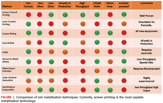
As a researcher and proponent of screen-printing technology (and, of course, an employee of one of the world’s top mass-imaging organizations), you may find it strange that I’m writing about alternative solar cell metallization technologies. But these other approaches do exist, and it’s important to understand them – and why many experts with no vested interest in screen printing still view the latter as the most viable, at least for the medium-term future.
Many alternative techniques have been around for a few years, and concurrent with their development has been the claim that one or more would displace screen printing as the reigning technology. So far that hasn’t happened, for two reasons: 1) Printer and paste manufacturers have kept pace with the latest demands for fine-line printing (we’re now sitting at 60µm wide lines in production and well below 50µm in a lab environment); and 2) the requirement for much thinner silicon (which would be subject to potential damage by the contact of printing’s squeegee pressure) to reduce cost has diminished in recent years, as the price of silicon has gone down by more than half.
Generally, the alternative metallization methods described below were applied to solar to reduce costs or to increase efficiency. In some cases, this was largely driven by the need to deposit material in a noncontact process to enable thinner silicon use. Each has its perceived advantages compared to screen printing (primarily noncontact techniques), as well as its drawbacks.
Laser transfer printing. This is a noncontact technology that uses a continuous tape loop and doctor blade arrangement to deposit paste, then locally heat the paste with a laser, which ejects the paste from the tape onto the wafer. Although nothing touches the wafer and the consumables costs are relatively low, this method cannot currently produce fine lines in high-volume manufacturing, and, consequently, the only viable market for it is for printing the back side of solar cells. Throughput is also fairly low.
Electroplating. This process – used also in semiconductor and printed circuit board fabrication – employs a chemical method to remove the silicon nitride locally, plate with a material (likely electroless nickel) to make the first contact with the wafer and electroplate the bulk copper on top of that. Because of copper’s corrosion problem, it then has to be passivated with a tin layer. The advantages of electroplating are the ability to produce ultra-fine lines with high conductivity and eliminate costly silver pastes. However, it does require three wet chemical processes that are time-consuming, labor-intensive, messy and waste-producing. This method also requires fairly high skills.
Seed print and light-induced plating. Either a screen- or an inkjet-printed low aspect ratio line is deposited with standard silver paste, and then silver is electroplated using the current generated by the cell itself during light exposure. In my view, the benefits of this technique are quite limited; there is a bit of extra conductivity from the silver because the electroplated silver is solid (as opposed to the honeycomb effect of fired silver paste), and there is reduced shadowing from the ability to plate narrow lines. But, the lines are limited to 50/60µm widths, which can be achieved already with screen printing. The disadvantages of a two-stage process, the additional capital expenditure for plating equipment, the line width limitations, and the chemical waste outweigh the marginal benefits.
Inkjet printing. This technology has been around for a long time and has various commercial applications. Initially, advocates thought it would be ideal for noncontact solar cell printing because of the historic success with inkjetting materials. But, inkjet printing requires low viscosity materials with nano-particles, so the paste is more expensive than traditional silver paste. Plus, most inkjet systems are challenged by high aspect ratio printing and need 10 to 20 passes to get the required height. The multiple passes obviously lower throughput significantly. There are also nozzle blockage issues. All in all, I think it’s very impractical for solar cell processing.
Aerosol or metal jetting. With aerosol or metal jetting, material is guided by pressurized gas and deposited onto the substrate. This method is noncontact, can do ultra-fine lines and has the positional accuracy of deposition. However, like inkjet printing, it is plagued by its inability to deliver high aspect ratios at high speed and also requires special inks.
Dispensing or extrusion. Automatic dispensing (also referred to as extrusion in some cases) for solar cell metallization is not that different from what is commonly used in electronics assembly. This is a needle dispensing technique where pastes are transferred in a non-contact method from the nozzle to the substrate. Dispensing is capable of achieving high aspect ratio line widths of 50µm, with further reductions likely, and has good positional accuracy. The drawbacks include the required use of special (read: expensive) pastes, nozzle blockage and low throughput.
Laser chemical metal deposition. Largely an experimental technique, laser chemical metal deposition is likely a few years away from any sort of commercialization. With this process, the solar cell is immersed in an electrolyte; a laser shines through the electrolyte, ablates an anti-reflective coating and causes activity in the emitter layer, which electroplates nickel lines. The advantages are its noncontact capability and the elimination of silver. If and when it becomes commercially viable, these advantages will have to be weighed against the associated waste, health and safety issues of a wet process.
Sputtering or evaporation. These technologies have been used in the semiconductor industry for a long time. Because they are semiconductor-accurate, extraordinarily fine lines and high aspect ratios can be achieved in a noncontact process. What’s more, just about any metal or stack of metals can be deposited. On the downside, sputtering and evaporation are very slow and require a high vacuum process. Throughput is adversely impacted by the requirement to have everything go through a vacuum chamber first. There are also tooling costs associated with making the photolithography resists used to define the plated or metal-coated areas. If this is achieved through a mask, then that is a tooling cost as well. Currently, the capital expenditure costs are high, but there is industry chatter about these techniques becoming more useful for backside aluminum.
So, there you have it: the pros and cons of screen printing alternatives to solar cell metallization. Currently, there is no other method that can deliver the aspect ratio or speed efficiency of screen printing. The technology’s inability to offer noncontact material deposition seems to be a moot point, if and until silicon wafer thickness begins to diminish. Even then, modern printing systems can effectively manage wafers as thin as 120µm with very low breakage rates. And while printing can’t eliminate silver pastes until there are fully functional, commercially available non-silver pastes, it can assist with reductions in silver consumption right now. Using print-on-print (POP) and dual print technologies, the cost impact of silver can be significantly mitigated. (“Strategies to Offset the Rising Cost of Silver,” "CIRCUITS ASSEMBLY, September 2011.) For the time being, I am of the firm opinion that screen printing is the most cost-effective, efficient method available for solar cell metallization.
[Ed.: To enlarge the table, right-click on it, then click View Image, then left-click on the table.)