Five principles form the basis for material selection and program decisions.
Over the years, the ESDA has regularly advised applying this principle to static control: keep it simple and keep it focused. Although technology, processes and materials have continued to evolve, the design and implementation of effective static control programs continue to be based on the following five concepts:
Design static protection into devices and products.
Eliminate static generating materials and processes.
Dissipate or neutralize static charges on process materials, equipment and personnel.
Provide physical protection from discharge events.
Measure processes and environment frequently to make sure everything is working correctly and make necessary corrections and improvements.
Design in protection. Our first principle is to design devices, products and assemblies to be as robust as is reasonable to the effects of ESD. Whenever possible, use less-static-sensitive devices or provide appropriate input protection on those ESD-sensitive (ESDS) devices that are used. The paradox here is that advancing product technology means further miniaturization and higher speed of operation that often are more susceptible to ESD and preclude the installation of protection devices at the chip level. However, the more ESD control that is built in to product design, the fewer problems later.
Eliminate and reduce generation. Obviously, product design isn’t the whole answer. You cannot get away from ESDS devices and other products that are sensitive to some form of electrostatic charge and discharge, but the generation and accumulation of electrostatic charge can be reduced to below the threshold of problems in most processes.
Start by reducing or eliminating static generating processes or materials, such as common plastics and other static-generating materials, from the work environment. ANSI/ESD S20.20-2007, “Protection of Electrical and Electronic Parts, Assemblies and Equipment (Excluding Electrically Initiated Explosive Device)” and IEC 61340-5-1-2007, “Electrostatics – Part 5-1: Protection of electronic devices from electrostatic phenomena – General requirements,” both require a careful review of the process areas to remove any unnecessary insulators. Because ESD does not occur between materials kept at the same potential or at zero potential, processes and materials in the work environment should be kept at the same electrostatic potential. Typically, these conductive or dissipative materials should be electrically bonded to the same common point ground, such as the verified utility or earth ground. In addition, provide ground paths with wrist straps, flooring, or work surfaces to safely reduce charge generation and accumulation on all personnel and conductive or dissipative items that enter the defined electrostatic protected area (EPA).
Dissipate and neutralize. Because all generations of static cannot be totally eliminated, our third principle is to safely dissipate or neutralize those electrostatic charges that do occur. Proper grounding and the use of conductive or dissipative materials play major roles. For example, workers who carry a charge into the work environment can rid themselves of that charge by attaching a grounded wrist strap or by stepping on a grounded ESD floor mat while wearing ESD control footwear. The charge goes to ground rather than being discharged into a sensitive part.
For some objects, such as common plastics and other insulators, grounding cannot remove an electrostatic charge. Typically, ionization is used to neutralize charges on these insulating materials. The ionization process generates negative and positive ions that are attracted to opposite charges on the surface of a charged object, thereby effectively neutralizing the charge. Use of dissipative materials for work surfaces and at the point of contact to a device can also be effective.
Protect products. Our fourth principle is to prevent discharges that do occur from reaching susceptible parts and assemblies. One way is to provide parts and assemblies with proper grounding or shunting that will dissipate any discharge away from the product. A second method is to package and store or transport susceptible devices in proper packaging and materials handling products. These materials may effectively shield the product from charge and discharges and reduce the generation of charge caused by any product movement within the container.
Proper packaging and materials handling not only provide protection within our own facilities and process, but may also provide protection when the final product reaches the consumer.
Measure and improve. Finally, measure your processes and environment. Don’t ask whether a process will create an ESD hazard and then guess at the answer; measure it. For example, use a fieldmeter to detect the presence of an electrostatic field that could pose an ESD threat. Measure the resistance to ground of personnel and process equipment. Measure the voltage accumulation on personnel and components in the work environment. Measurement is a win/win situation. Identify and quantify those areas that really do need static protection, so focus can be on those areas that are of the greatest concern. In addition, you can identify areas that do not pose an ESD hazard, saving you the expense of providing unneeded protection.
These five principles form the basis for effective static control programs. They aid in the selection of appropriate materials and procedures to use in effectively controlling ESD. In most circumstances, effective programs will involve all these concepts. No single procedure or product will do the whole job. In developing control programs, identify the devices that are susceptible, their level of susceptibility, and those operations that pose an ESD hazard to them. Then ask which of these concepts will protect these devices. Finally, select and implement the combination of procedures and materials that accomplishes the task.
References
1. ESD Association, 7900 Turin Road, Bldg. 3, Rome, NY 13440, 315-339-6937, esda.org. 2. IEC – International Engineering Consortium, iec.org.
This column is written by The ESD Association (esda.org); This email address is being protected from spambots. You need JavaScript enabled to view it..
A recent survey of more than 450 PCB designers reveals how designers benchmark their tools.
Good news, CAD vendors: Your customers don’t hate you. So says an October survey conducted by PRINTED CIRCUIT DESIGN & FAB. The two-week-long survey asked hundreds of printed circuit board designers, design engineers and other layout specialists how they use and think about various CAD tools.
The survey was spurred by a question posed by veteran PCB designer Bill Brooks, who asked, “What sort of data is available to benchmark the top four CAD tools out there?” What we learned might surprise some readers.
Despite the occasional rant, designers actually do like their CAD vendors, with the heavy majority giving high marks for service. But when it comes to selecting a tool, some of the features heavily pushed by vendors – autorouting stands out – are not as important as such fundamental if less sexy features like the parts library or even the GUI.
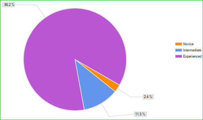
First, some notes about the demographics: Of the 451 designers who completed the survey, 86.2% consider themselves to be “experienced,” while 11.3% are in the “intermediate” stage of their career. Only 2.4% are “novices.”
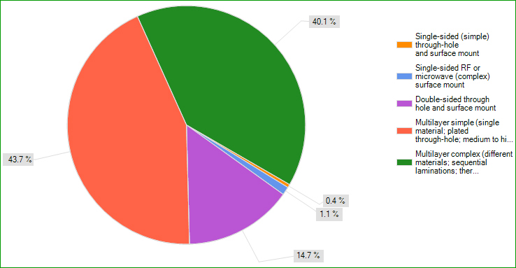
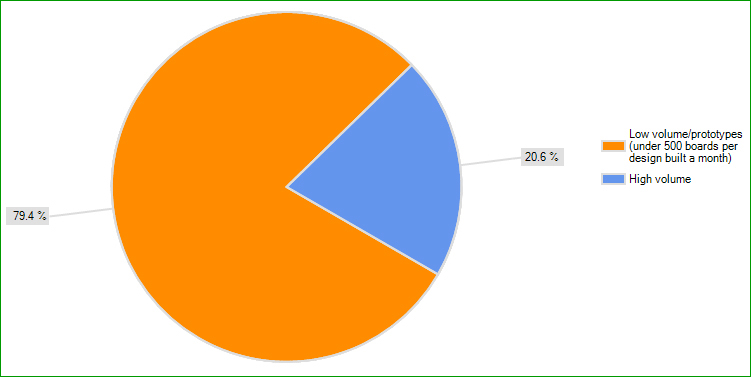
Most of the respondents primarily design multilayer boards (four layers and up). Nearly 44% say they typically design multilayer “simple” boards, while 40.1% design multilayer “complex” boards. Smaller percentages say they typically design single-or double-sided through-hole and surface mount boards (Figure 1). A large percentage (79.4%) say they design mostly low-volume/prototype boards (under 500 boards per design built a month), while 20.6% design high-volume boards.
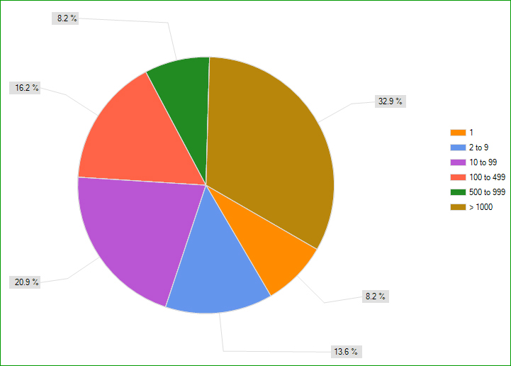
Almost a third of respondents work for large firms; 32.9% say their company has more than 1,000 employees. Another 8.2% work for firms with 500 to 999 employees; 16.2% say 100 to 499, while 20.9% say their company employs 10 to 99. Only 13.6% of those responding work for firms employing two to nine employees; 8.2% employ one employee.
[Ed.: To enlarge the image, right-click on it, then click View Image, then left-click on the table.)
FIGURE 1. Type of board typically designed (n = 451).
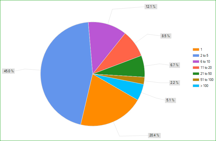
While the designers’ companies have a large number of staff, the number of PCB design tool users within each firm (not just at their site) is small. Forty-five percent of respondents say the company has a total of two to five design tool users, and 20.4% say only one user. Another 12.1% say six to 10; 8.5% have 11 to 20; 6.7% say 21 to 50, and 2.2% have 51 to 100 design tool users in the firm; 5.1% say more than 100 users.
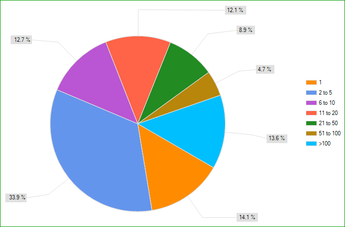
Schematic users in the company vary from one (14.1%); two to five (33.9%); six to 10 (12.7%); 11 to 20 (12.1%); 21 to 50 (8.9%); 51 to 100 (4.7%), and more than 100 (13.6%).
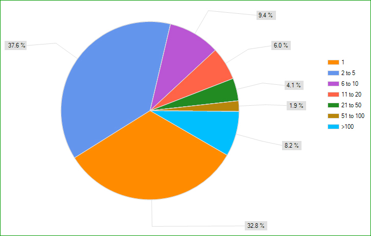
Circuit simulation users within the company are few, with about 70% having five or fewer. Some 9.4% of firms have six to 10; 6% have 11 to 20; 4.1% have 21 to 50; 1.9% have 51 to 100, and 8.2% have more than 100.
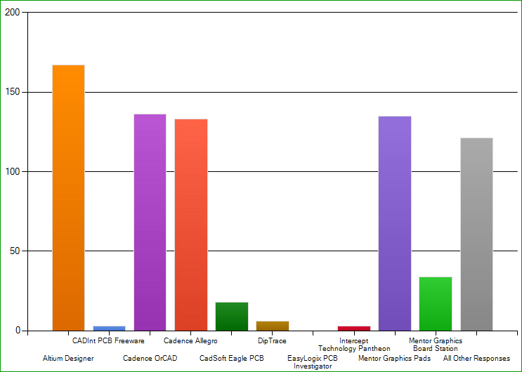
While the three largest CAD tool providers by revenue are Mentor Graphics, Zuken and Cadence, the respondents didn’t match up so neatly. Indeed, Cadence, Mentor Graphics and Altium users were most represented, with about 63% using OrCad or Allegro, 31.7% using Pads, and 39.2% using Altium Designer (Figure 2). Another 19% use Expedition, while 8% use Board Station. (Users were allowed to list more than one tool.)
FIGURE 2: CAD tools currently used (respondents could choose more than one answer).
Just under 10% of the respondents indicated they use Zuken’s CR 5000, CADStar or CR 8000. Other CAD software such as CadSoft Eagle PCB, DipTrace, Intercept Technology Pantheon, and CADInt PCB Freeware received small percentages.
Not surprisingly, board designers are busy. When asked how many new designs they complete per year, 21.4% indicated more than 25 (Figure 3), and another 13% design 15 to 25 boards.
FIGURE 3: New board designs per year (not including respins).
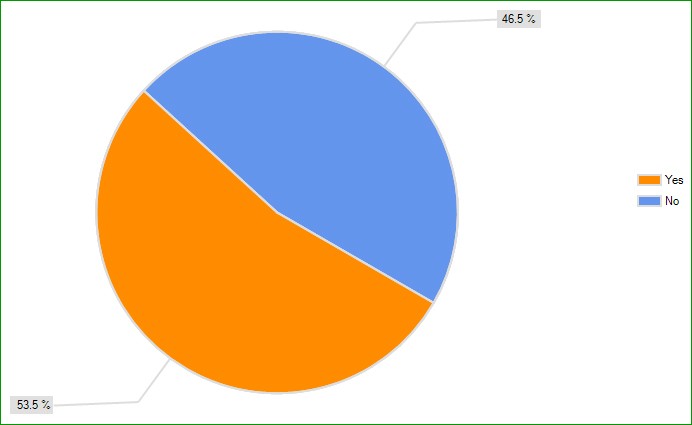
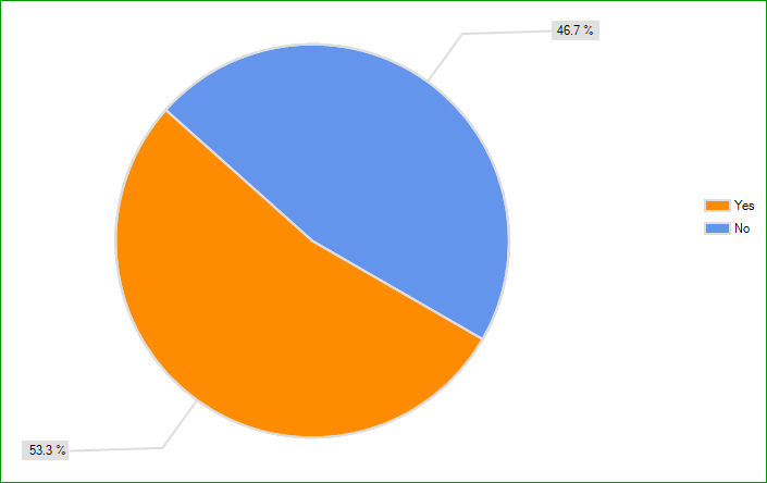
Slightly more than half the responding firms (53.5%) have librarians who manage their CAD libraries, according to the survey, and slightly more designers (53.3%) design PCBs with high density interconnects than those who don’t.
The main reason for the survey was to gauge how designers feel about their primary tools – and tool provider.
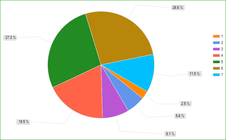
One might not believe this from user message boards, but designers are generally happy with their primary vendor’s customer service. They were asked to rate the service on a scale of 1 to 7, with 1 being “poor” and 7 being “excellent.” Nearly 54% of respondents rated their vendor a 5 or 6, and another 11.5% of designers gave them a 7. Just 16% rated their vendor as a 3 or less.
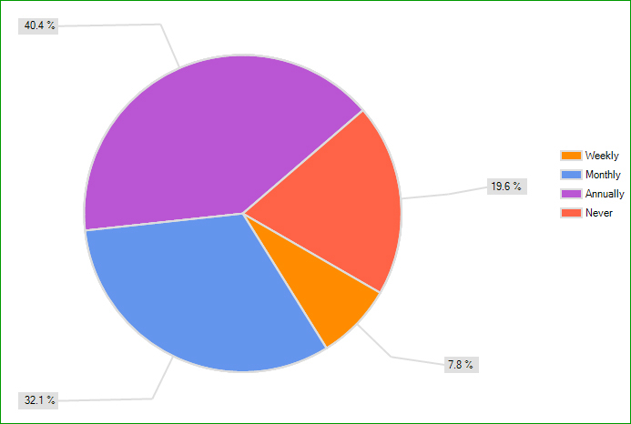
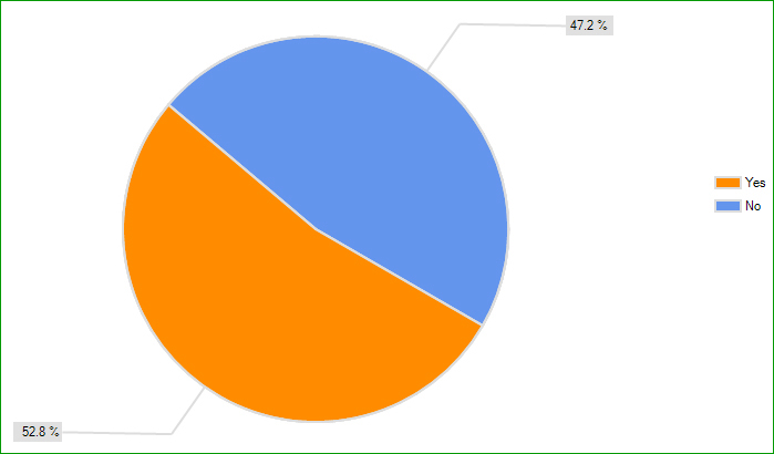
A little more than half of survey respondents (52.8%) say the primary tool vendor’s customer/technical support is worth the expense. Designers say they most often use vendor support annually (40.4%) or monthly (32.1%), with few using it weekly (7.8%); 19.6% say “never.”
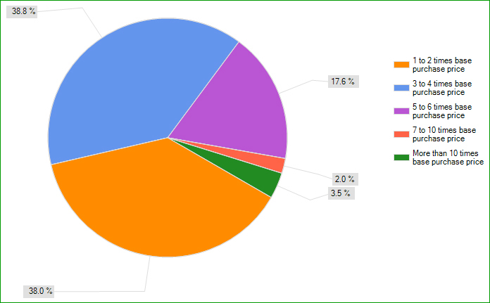
Designers were asked to estimate the total cost of ownership to produce successful PCB designs (purchase price, maintenance, training, libraries, process development, interfaces, etc.). It was basically an even split between one to two times and three to four times the base purchase price (Figure 4).
FIGURE 4: Total cost of ownership to produce a successful PCB design, relative to the tool base price.
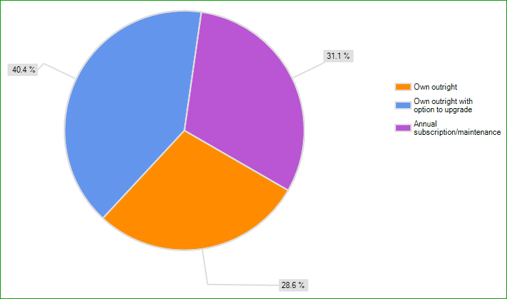
Designers would prefer to own their design tools outright (69%), with 40.4% of those saying they’d also like the option to upgrade. Slightly more than 31% of respondents say they’d prefer an annual subscription that includes maintenance.
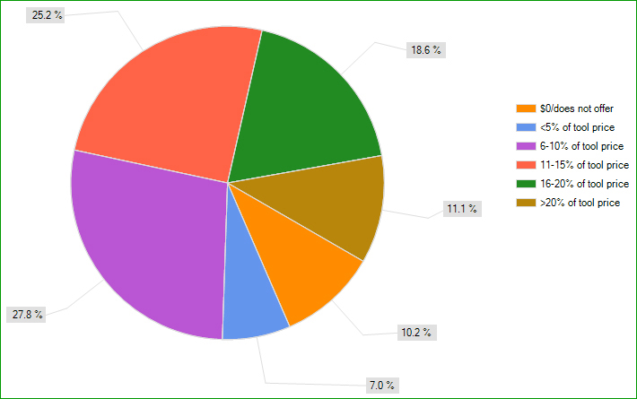
When asked how much primary tool vendors charge for support and maintenance, the most common response was six to 10% of the tool price (Figure 5). However, few charge less than that: A combined 17.2% charge 5% or less for support and maintenance or don’t offer it.
FIGURE 5: Typical maintenance and support add-on charges.
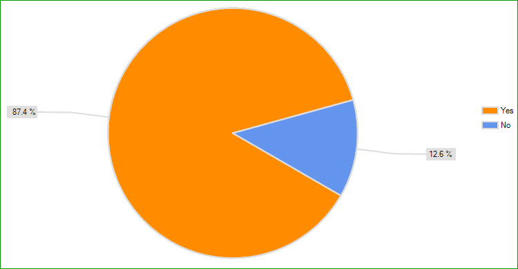
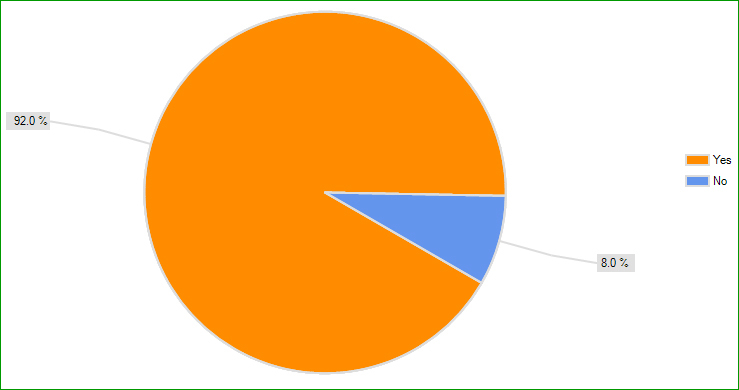
A substantial number of designers use their primary EDA/CAD tool for analog design (87.4%), and a significant 92% use their primary CAD tool for digital design.
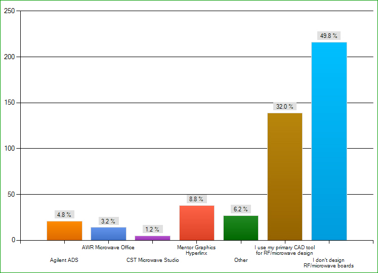
While almost half of respondents (49.8%) say they don’t design RF/microwave boards, of those who do, one-third say they use their primary CAD tool for such designs. Other responses include Mentor’s Hyperlinx (8.8%), Agilent ADS (4.8%), AWR Microwave Office (3.2%), and CST Microwave Studio (1.2%).
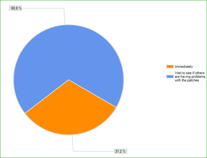
Designers aren’t quick to install upgrades, with 68.8% waiting to see if others have problems with the patches first.
… But Not Necessarily Their Autorouters
Designers were asked to rate a series of criteria in terms of their importance in a PCB design tool. Here’s how the answers stacked up:
Most designers say design reuse is either very important (37.8%) or moderately important (38%). Another 16.9% were “neutral.”
Designers are divided on the importance of concurrent design, or different areas of the board designed in parallel. Only 17.1% say it’s very important, while 24.5% believe it to be moderately important, and 23.1% say it’s of little importance. The “not considered” category received 11.5% of responses.
Constraints (high-speed design rules, impedance, skew, topology, etc.) are high on the designers’ list, with 59.2% saying they are very important. Another 25.7% say they are moderately important. The rest of designers are “neutral” on the subject (9.7%), think they aren’t important (4.3%), or don’t consider them (1.1%).
A small number of the designers who responded to the survey find autorouting speed to be a very important feature of their CAD software (6.1%). However, 22.6% say it is moderately important, while 25.7% are neutral on the topic. Another 21% say it is of little importance, and 24.6% say it is “not considered.”
Autorouting accuracy is a somewhat different story, as 28.9% find it to be very important; 16.9% say moderately important; 16.3% are “neutral”; 12% say it is of little importance, and 26% responded “not considered.”
About 68% of designers say analysis features are either very important (27.6%) or moderately important (40.5%). Another 21.5% are neutral, while 10.4% either don’t believe they are important or don’t consider them.
DfM/DfT/DfA support is a priority, as more than 75% of designers list it as either very important (38.7%) or moderately important (36.4%). Less than 10% say it’s not important or don’t consider it.
Respondents find ease of design visualization another top priority, with 87.5% saying it’s either very important (51.7%) or moderately important (35.8%). A small percentage are neutral on the topic (11.1%), and only 6 of the 451 designers say it’s not important or “not considered.”
Also a priority is the ability to integrate with other EDA tools. Nearly 77% of designers say this is very important (40%) or moderately important (36.9%). Only 5.6% responded with “of little importance” (4.1%) or “not considered” (1.4%). Another 17.6% are neutral.
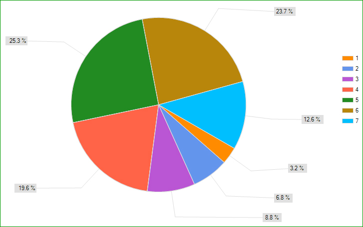
More than 91% of designers find ease of data importing/exporting to be very important (65.9%) or moderately important (25.3%).
Library creation is also paramount, with more than 93% listing it as very important (75.1%) or moderately important (18.2%).
Placement is another key element in PCB design software. Nearly 90% of designers say it’s very important (61.6%) or moderately important (28.2%).
A whopping 96.2% of respondents think user interface is very important (75.4%) or moderately important (20.8%).
Yet another important feature is manual/interactive routing, with 89.4% finding it to be very important; 8.3% say moderately important.
Design rule definitions also top the list, with 97.3% of survey respondents saying they are very (78.6%) or moderately important (18.7%). Design rule verification is also a high priority, with “very important” (82.7%) and “moderately important” (14.4%) eclipsing other responses.
Answers for mechanical and documentation capabilities were split between very important (46.3%) and moderately important (43.8%). Only 1.8% find them to be of little importance, while 7.2% are neutral.
What is apparent is that designers tend to agree on the important features they want out of their CAD tools, specifically DfM/DfT/DfA support, ease of design visualization, integration with other EDA tools, user interface, data importing and exporting, and library creation, to name a few. We did not ask how often designers change tools; that might be something to ask next time. It will be interesting to see if these numbers shift over time.
FIGURE 6. PCB design experience.
FIGURE 7. Number of employees.
FIGURE 8. Firms’ PCB design tool users.
FIGURE 9. Firms’ schematic users.
FIGURE 10. Firm’s circuit simulation users.
FIGURE 11. Company librarians who manage CAD libraries.
FIGURE 12. Volume of boards designed.
FIGURE 13. HDI used to design PCBs.
FIGURE 14. Primary EDA/CAD tool used for analog design.
FIGURE 15. Primary CAD tool used for digital design.
FIGURE 16. Preference for tool ownership.
FIGURE 17. Frequency of primary tool vendors’ customer/technical support.
FIGURE 18. Is primary tool vendors’ support worth the expense?
FIGURE 19. Upgrade installation.
FIGURE 20. RF/microwave design software tool.
FIGURE 21. Ratings for primary vendors’ customer service (1 = poor, 7 = excellent).
FIGURE 22. Satisfaction with vendors’ customer service (1 = poor, 7 = excellent).
Chelsey Drysdale is senior editor of PCD&F (pcdandf.com); This email address is being protected from spambots. You need JavaScript enabled to view it..
Are they ever OK? Our columnist has an emphatic response.
The answer to the question “Is it ever okay to put open vias in BGA pads?” is simply “no.”
It’s no, no, no, no, not ever!!! That makes it easy. No technique to worry about. No tolerances. Nothing. Just don’t put an exposed via in a BGA pad. The only option is between the pads, with a complete solder mask dam between the pad and via, or have the vias filled and plated over at the board house. It doesn’t matter if the BGA is sub-millimeter pitch or larger-than-millimeter pitch. Nothing but metal is allowed on the BGA pad.
Now, other components offer more flexibility and thus require some choices and guidelines. Reader Andy B. asked about large components, such as voltage regulators, where the manufacturer has recommended vias to connect the thermal pad to the ground plane, or to additional thermal area on the back side of the PCB.
The easy answer is to just treat it like a QFN and read our various suggestions1 surrounding that form factor. Having the extra room does allow for additional flexibility, but if the vias are open, they still run the risk of sucking solder to the other side of the PCB. You can sometimes get away with really tiny vias.2 But it’s not best practice.
It’s really a matter of tradeoffs. Some say to never fill or cap the via because doing so might impede the thermal transfer. Well, power chip manufacturers, you shouldn’t rely on unbuildable design to meet product specs. Vias can be filled with thermally conductive material. Or the via can be capped with solder mask.2 Just make the via cap as small as possible – 100 to 125µm larger than the via.
Finally, segment the paste stencil layer. Solder paste on top of an open via or even on top of a masked via could be asking for trouble. In this power MOSFET footprint (Figure 1), there are four vias (which will be capped) between the openings of the stencil under the part. The original copper stops at the blue dashed lines. I’ve added the extra thermal area as a copper pour with vias to give additional cooling area, another technique sometimes used with power parts. The vias in the extra thermal area do not need to be filled, as they are in the solder mask covered area, not the paste covered area.
Ed.: Read Duane’s blog each week at circuitsassembly.com/blog.
References
1. Duane Benson, “Large Via In Pad,” June 11, 2010, circuitsassembly.com/blog/?p=992. 2. Duane Benson, “Open Small Vias,” Sept. 21, 2011, circuitsassembly.com/blog/?p=2195.
Duane Benson is marketing manager at Screaming Circuits (screamingcircuits.com); This email address is being protected from spambots. You need JavaScript enabled to view it.. His column appears bimonthly.
The Japanese Ministry of Economy, Trade and Industry (METI) released September’s production data for the electronics industry in Japan. A nine-month snapshot for the first three quarters is now available, and allows us to review a few market trends and assess our plans for the remainder of the year.
Design considerations for moving from 0.5mm pitch to 0.4mm pitch and below.
Package-on-package is a method of stacking components atop one another. Some OEMs use PoP to reduce the board real estate area, particularly for small handheld products and devices. Others are moving to PoP because end-markets demand greater performance in smaller systems and products. In either case, OEMs will find that there’s a game changer going from 0.5mm pitch BGA PoP to the next generation, 0.4mm ultra-fine pitch BGA PoP.
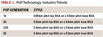
Industry trends say that PoP-populated PCBs will evolve in three stages as shown in Table 1.
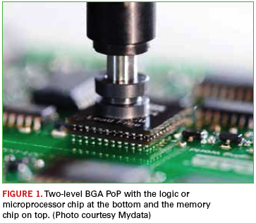
Currently, in some camps, PCB designers are at the first stage using two-level BGA PoP with the logic or µP (processor) chip at the bottom and the memory chip on top (Figure 1). However, there are certain key steps involved in increasing success at the third level. But first, before stepping out with 0.4mm pitch BGA PoP-based PCB designs, it’s important to revisit those rules-of-thumb at the 0.5mm level and above. These rules-of-thumb relate to pad sizes and solder mask openings up to 0.5mm pitch.
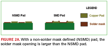
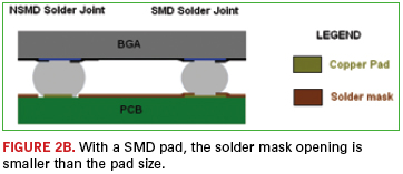
First is to maintain pad size around 85% of the ball size of the BGA. Second is to provide a non-solder mask defined (NSMD) pad whereby the solder mask opening is larger than the NSMD pad (Figure 2a). Typically solder mask is opened to a diameter of around the ball size of the BGA. In this instance, the solder mask is recessed, permitting it to provide stress relief to the NSMD pad during reflow. In short, it creates a protective dam so that solder can go around it.
Further, since there are no existing published design guidelines for 0.4mm pitch PoP-based PCBs, be wary of today’s conflicting reports. Issues stemming from these reports deal in large part on PCB pad sizes and solder mask openings. Take, for example, a 0.4mm pitch BGA PCB design using NSMD pad sizes, where in a low-volume run the results were highly acceptable. However, for larger production, this approach produced low yields. By adopting the solder mask defined (SMD) pad approach (Figure 2b), whereby the solder mask opening is smaller than the pad size, better yields and results are achieved. Also, it’s important to note when deploying NSMD pads for 0.4mm and 0.3mm pitch BGA/PoPs, the chances are great of creating bridging between pads due to insufficient solder mask webbing between pads.
Key Factors to Pursue
Since 0.4mm pitch BGA PoP-based PCB design is in its infancy, it is a good idea for the PCB designer to perform preliminary experimental layouts and prototype rounds to get the lay of the design before launching into a full-fledged layout. Rules followed for 0.5mm pitches may not work for 0.4mm cases at high volumes. Typically, ball sizes of 0.4mm pitches are smaller. Reducing the pad size by another 15% may make the solderable area insufficient. Second, using NSMD with 0.4mm parts may cause bridging between adjacent pads. Third, since the pad sizes are so small, and there is no solder mask webbing to provide adhesive strength, it may peel off during reflow or in the field.
Against this backdrop, there are six key factors affecting the reliability of a 0.4mm ultra-fine pitch BGA/PoP-based PCB design. Those are pad design, via-in-pad guidelines, via finish, stencil design, solder paste, and thermal profile.
As suggested, SMD is the pad of choice for 0.4mm pitch. In this case, the pad is created as the same size of the BGA ball. Solder mask opening is around 15% less than the ball diameter. Here, the solder mask laps over the edge of the copper pad to strengthen the connection in a couple ways: One, it strengthens the bonding between the copper and the PCB’s laminate; two, with the copper pad going farther into the solder mask, copper area is larger. That larger copper area provides a greater surface for the PCB laminate to adhere, making the connection twice as strong.
Also, in these designs, traditional BGA dogbone fan out used for larger pitches with extended real estate is not considered at all. Instead, via-in-pad is used, a specialized technique for escape routing fine-pitch BGAs. Before discussing guidelines for use, it’s a good idea to revisit the via-in-pad approach. This escape routing technique involves vias being placed directly on the BGA pads and filled with a conductive or a nonconductive material, which provides a fairly flat surface. Traditionally, silver was used to fill the vias, and a small increase in density was realized so that the designer could route a few more signals on the outer surface. That technique has evolved considerably, and now the materials of choice fall in the nonconductive category. The reason: Vias filled with a nonconductive epoxy perform better because the coefficient of thermal expansion (CTE) is comparable with that of the PCB.
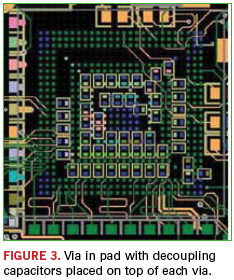
Therefore, the rate of expansion is similar to the board material, allowing for a more reliable joint. Issues like via out gassing and solder voids can be avoided. The same method of filling vias is used on 0.4mm PoP designs. A key point to make is that whenever there are vias below a BGA and available for connection, they should be filled, tented, or capped. Otherwise, they can cause voids and out-gassing during reflow. Also, as shown in Figure 3, discrete decoupling capacitors can be placed directly over the vias on the bottom side. This provides a low inductance path to the power system.
Place and Route
When it comes to 0.4mm pitch BGA PoP, it’s not a good idea to place a BGA on the opposite side of another BGA, which is the typical case in 0.5mm pitch BGA and above. Instead, BGA/PoPs should be placed offset from each other with about 500 mils spacing to maintain board level reliability and ease of debugging on the bench when needed.
Again, since 0.4mm pitch BGA/PoPs are so new, manual routing is recommended over autorouting. Reason: An autorouter is a computer program based on mathematical algorithms and fixated on making connections. It doesn’t think like a human designer. In most instances, using the autorouter results in unusual traces, many unnecessary vias routed and many unnecessary loops.
In effect, the autorouter creates more vias than are required, thus reducing the reliability of the final assembly. Also, those extra vias add discontinuities if the design calls for certain impedance requirements. Typically, impedance is based on the geometry of the connection from driver to receiver. Hence, that impedance path needs to be uniform. Whenever there is a via, there is a discontinuity in that uniform pad, and impedance changes at that particular moment. Ideally, for a 0.4mm pitch BGA/PoP-based design with high-speed signals, you don’t want a via. Additional vias will cause considerable discontinuities and subsequent ringing and reflections.
While performing the routing, it’s also vital to avoid creating heat sinks. How can a designer inadvertently do this? This occurs when a trace is put on a via or a dogbone fan out is performed from a via that’s almost the same size as the pad. The result is the traces and vias pull heat away from the BGA/PoP and cause issues during assembly. In another example, copper pour is placed over BGAs. This may happen when there are multiple power/ground pins on the device. During assembly, this arrangement will sink the heat during reflow and cause cold solder joints, resulting in opens or intermittent connections.
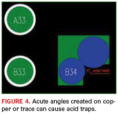
Also, in the realm of routing, acute angle traces should be avoided when connecting BGA pads, as they could result in acid traps. Acid traps are acute angle areas or small areas where etching chemicals get stuck, and eventually, those small chemicals eat away the traces and intermittent connections result (Figure 4). Finally, the designer should design with metric units rather than English for fine-pitch BGA devices and PoP. This will not only increase accuracy, but will also avoid requiring four decimal places of accuracy when converting from micrometers to mils.
Team Effort
There’s always talk about working together to successfully complete a project. But in the case of 0.4mm ultra-fine pitch BGA/PoP-based PCBs, there is no question it is essential that the PCB designer, fabricator and assembler work in unison, with the designer taking the lead. The PCB designer must maintain regular discussions with the fabricator to understand its capabilities, such as determining whether it can handle certain minimum hole size aspect ratios. Part of that dialogue includes understanding the spacings for a high-speed design’s impedance control traces, and knowing the chosen substrate material’s capacity to handle those requirements. Furthermore, the designer must have a good handle on a fabricator’s manufacturing limits. Those can be divided into three categories: standard technology, high-yield, and engineering development. The first refers to a fabricator’s capability, for example, 5 mil traces and spacing, which is a midrange capability for most board shops today. For mass production, high yield is typically 8 mil lines and spaces. (These numbers are relative, so for some fabricators, 10 mils will be high yield, while 8 mils might be typical for others.) Third, there’s the engineering development category. This deals with a fabricator’s highly advanced capabilities, which fall into the 2.5 mil traces and 2.5 mil spacing class.
The layout designer must also know the assembler’s capabilities, such as the minimum pitch that assembler can work with. Either it can or cannot perform 0.4mm ultra-fine pitch BGA/PoP PCB assembly. If it is building 0.4mm pitch, what kind of solder paste are they using? Are they following manufacturer’s recommendations on the reflow profile? The designer must also have discussions with the paste manufacturer to ensure the right pad sizes are associated with the right solder paste. Avoiding warpage is another key area demanding close interaction between the designer and assembly. By not paying special attention in this area, excessive warpage can result in bridging, solder slumping, head in pillow, or opens.
PoP is an emerging technology, and will be utilized more as the industry gears toward further miniaturization of the existing technologies. Do not assume that the same techniques that work for larger versions will necessarily scale to the smaller ones.
IPC’s new president has put the attention back where it belongs: on member needs.
Want to know how new IPC president John Mitchell is? He still calls members “customers.” It’s, as they say in Las Vegas, a “tell,” a verbal tic that gives away what someone is thinking.
In this case, that’s a good thing. When we met with Mitchell in the IPC offices in Bannockburn, IL, on Aug. 9, he wasn’t quite four months officially into the new job. But over the course of our conversation, the former Bose and Alpine Electronics executive quickly showed where his head is at, stressing repeatedly that the 55-year-old association needs to refocus on its members.
At that point, Mitchell had spent much of his first few weeks visiting OEMs, fabricators and EMS companies, asking again and again, “What are your big challenges?” Most ticked off two to seven items each, for an aggregate 35 issues, of which 30, he said, IPC has some effect on. That list now becomes the battery for the IPC engine. “Where we put our effort is where we can help,” he says.
IPC has come under criticism from many quarters over its insular nature and brusque relations with other organizations and even some members. Mitchell, who comes across as highly detailed and involved, did not shy away from that discussion. In fact, he capitalized on it. Recognizing the IPC culture needed to reposition from how to grow IPC to how to help the members, Mitchell has restructured the organization to better underscore the notion of IPC staff member as account representative. “We help IPC members realize the benefits IPC can give them. We need to be local in feel.”
Not that every program needs an overhaul. Mitchell noted the strengths of the technical programs and trade shows as two areas that are functioning properly. “IPC has done some pretty good things. We have some good basic stuff. The standards provide commonality across the globe.”
Likewise, the Apex Expo exhibition is a “great thing”, he says, although improvements are always possible. Mitchell, who has two decades’ experience in consumer electronics, noted that the CES attracts the entire chain from designers to supplier to customer. “It’s a massive meeting of the industry, where we can accomplish a great deal.” He wants Apex Expo to accomplish that same lofty goal, suggesting daily “themes,” such as medical, automotive and consumer to appeal to a wider audience.
One area IPC has encountered challenges is in meeting the demands of a wide variety of constituents, some of whose needs are in conflict. Mitchell is quick to acknowledge addressing those tensions won’t be simple. “There are different benefits IPC needs to provide to different-sized organizations. We need to be flexible enough and listen to the members to do this well. For the smallest companies, I don’t know the best way to help them yet, but we will figure it out.
“I have to provide 10 times the value, 100 times the value, whatever it is. That’s how we’ll determine what we should be doing. Does it add value to our members? It shouldn’t be only for the benefit of IPC. It’s all about providing member value.”
An engineer by education and training, he is optimistic, however, about how the technology can both bring members together and present an unbounded future. “Printed electronics is an awesome opportunity for growth in the US. The industry can get together with graphics manufacturers and raise their expertise and find new markets. Our job is to transfer technology and information on the importance of that technology.”
Other opportunities, he adds, for IPC to help its members include market research and government relations. “It’s not just about only doing things for the future, it’s about helping the current business situation. We look at how to close the gap.”
Our conversation turned to working with other associations, something IPC has occasionally struggled with. Mitchell said, “Associations don’t have to function like businesses and be competitive with each other. There are huge collaboration opportunities.” Interestingly enough, two months later, he agreed to move IPC’s semiannual task group meetings to SMTAI, a move that will firm up support of the latter event, while saving time and money for countless IPC members.
Government relations are another complicated area. IPC’s membership is worldwide, and many MNCs either have their own lobbyists or are reluctant to support efforts that might hamper their competitiveness outside the US, facts Mitchell readily acknowledges. “It’s largely about the medium and smaller organizations. GR is tricky for IPC. We can’t say, ‘We will fight an issue that will only help US manufacturers.’ But global issues, we can go after these. Conflict minerals – even though that is US-focused, the MNCs want to build one product that is used everywhere. We mobilize when we can bring science to the issue.”
Mitchell’s enthusiasm and thoughtfulness make him the right person to lead IPC, and he’s ready for the challenge. “We’ve got a good foundation. We are in a very stable position. Here, we have opportunities to serve our members.”