A host of new specifications aims to overcome coverage issues brought on by high-speed circuits.
The influx of high-speed signals on boards, and the challenge to the test environment, has invigorated interest in limited access methodologies such as boundary scan and built-in self-test (BIST). The industry is gearing toward adopting key initiatives to IEEE standards, so as to be able to help resolve these test challenges. The following are the proposals to extend IEEE Standard 1149.1 boundary scan capability into embedded testing, as well as the BIST currently in use by OEMs in the semiconductor and board design areas.
IEEE P1687
The challenge. Board assemblies increasingly are populated with high-speed semiconductors and memory in the GHz range. As a result, placing testpoints on the PCB traces is nearly impossible, as it would degrade signal integrity. Without these testpoints, manufacturers will no longer be able to use ICT to capture defects such as opens, shorts and wrong component values. In turn, this would increase test and overall manufacturing costs.
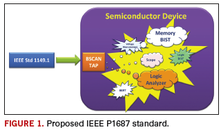
The proposed solution. OEMs and EMS providers are well aware of these challenges. Their need for a viable solution paved the way for the surge in interest in the IEEE P1687 standard, also known as Instrument JTAG or iJTAG. The objective of iJTAG is to develop a method and rules to access the instrumentation embedded into a semiconductor device without the need to define the instruments or their features using IEEE Standard 1149.1. The proposed standard would include a description language that specifies an interface to help communicate with the internal embedded instrumentation and features within the semiconductor device (Figure 1).
The purpose of the P1687 or iJTAG initiative is to provide an extension to IEEE 1149.1 specifically aimed at using the TAP to manage the configuration, operation and collection of data from this embedded instrumentation circuitry.
The benefit. With the proposed IEEE P1687 standard, test equipment providers will be able to access the embedded instruments in the semiconductor devices for testing purposes. At the same time, electronics manufacturers will be able to regain test coverage with minimal cost impact by integrating this solution into their current test process. Here are some ways in which P1687 can be implemented on the manufacturing floor:
1. Integrated into existing ICT. 2. ICT system > P1687 test solution. 3. P1687 test solution > functional test. 4. Integrated into existing functional test.
Among the possible implementations for P1687, integration into the ICT system would most benefit manufacturers, as the majority of high-volume companies use ICT to screen structural defects. With this implementation, EMS companies would be able to increase the value of their ICT and avoid a costly investment in another system to cover both the analog and digital defects of the assembly.
IEEE P1581
The challenge. One of the most common devices today is Dynamic Data Rate (DDR) memory, which can be found on everything from netbook motherboards to a larger high-end server and telecommunications boards. The challenge in testing memory devices lies in the high clock speeds for DDR memory, which now run in the GHz range. Again, with such clock speeds, testpoints would no longer be viable. The lost coverage means failures could only be captured after ICT, where finding defects and repairing them would be five times more costly.
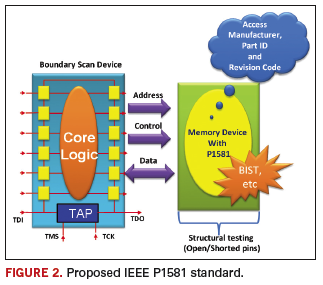
The proposed solution. The proposed IEEE P1581 (Figure 2) aims to develop a standard method for testing low-cost, complex DDR memory devices, which would be able to communicate through another semiconductor device with an IEEE 1149.1 boundary scan capability. Presently, even if DDR memory devices adopt the IEEE 1149.1 boundary scan standard, this is still not a feasible test, as it will require the addition of the four mandatory TAP pins to the DDR device, which would add to the devices’ complexity and cost. P1581 would provide the protocol to access the test mode within the memory devices, without the need for dedicated test pin requirements. The defined standard for this new test technology would enable each vendor to create its own method for implementing test hardware functionality in memory devices. It guides them on the necessary implementation rules for access and exit test modes. In contrast to IEEE 1149.1, this standard provides a static test method and requires fewer test pins. The standard would also allow implementation of P1581 on other semiconductor devices besides memory devices.
The benefit. P1581 would help the DDR memory vendor to enable its memory devices to communicate with boundary scan-enabled devices. Manufacturers would regain the test coverage on DDR memory that even current standalone solutions like 1149.1 are finding hard to run with any good measure of stability due to high clock speeds.
IEEE 1149.8.1
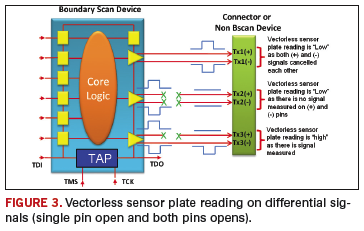
The challenge. High-speed differential signals, commonly known as SerDes (serial/deserializer) are reason to remove testpoints on assemblies. ICT has seen innovations to regain test coverage on connectors and devices connected to boundary scan devices without the need for testpoints by using a combination of boundary scan devices as signal driver and a noncontact signal sensing or vectorless sensor plate to detect opens and shorts on connectors, sockets and semiconductor device pins. However, this solution still falls short of being able to provide 100% coverage on differential signals. An example of failure escaping detection is when both differential signals (Tx+ and Tx-) are open, but the detected measured value of vectorless sensor plate will still be the same when both signal pins are properly soldered (Figure 3).
The proposed solution. IEEE 1149.8.1 entails a selective AC stimulus or differential signals, which when combined with noncontact signal sensing or a vectorless sensor plate, will allow testing of the connections between devices that adhere to this standard and circuitry elements such as series components, sockets, connectors and semiconductor devices that do not implement IEEE 1149.1 standards.
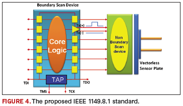
This standard specifies extensions to IEEE 1149.1 that define the boundary-scan structures and methods required to facilitate boundary scan-based stimulus of interconnections to passive and/or active components. This standard also specifies Boundary Scan Description Language (BSDL) extensions to IEEE Standard 1149.1 required to describe and support the new structures and methods (Figure 4).
The benefit. IEEE 1149.8.1 would enable selective AC stimulus generation that, when combined with noncontact signal sensing, would allow testing of signal paths between devices adhering to this standard and passive and/or active components. The biggest benefit of 1149.8.1 is that there is already a working solution currently implemented in some ICTs using a noncontact signal sensing or vectorless sensor plate that detects open/shorted pins on non-boundary scan devices and connectors connected to boundary scan devices.
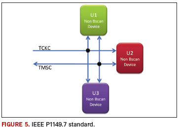
IEEE 1149.7
The challenge. Assemblies, especially those used in consumer products, are pressured by shrinking form factors. In recent years, we have seen implementation of multi-core system-on-chip (SoC), multi-die packages on system-on-package (SoP), and package-on-package (PoP) devices. All these technologies pose new challenges when it comes to manufacturing test due to limited testpoints and higher speed. This is causing existing manufacturing test systems to lose test coverage, even with the implementation of IEEE 1149.1.
The proposed solution. IEEE 1149.7, also known as compact JTAG or cJTAG, is compatible with the traditional IEEE 1149.1 (JTAG) standard to provide an enhanced test and debug standard that meets the demands of modern systems. One unique feature of 1149.7 is the reduced pin count interface for the test access port (TAP) interface; it uses a two-wire interface, versus the traditional 1149.1 four- or five-wire TAP interface. Since IEEE 1149.7 is compatible with 1149.1, this proposed standard also permits four- or five-wire implementation (Figure 5).
With the adoption of a two-wire interface on IEEE 1149.7, devices on the IEEE 1149.1 standard will benefit from this, as it makes it easier for boundary scan to be implemented on complicated new package technologies such as SoC, SoP and PoP, which does not implement 1149.1 boundary scan chain using the standard four or five-wire TAP interface.
The benefits. IEEE 1149.7 would enable easier implementation of IEEE 1149.1 for SoC, SiP and PoP. IEEE 1149.1 implementation is limited to boundary scan chains, as it requires the connection of every TAP interface of every boundary scan device targeted for testing. In comparison, IEEE 1149.7 would simplify this by enabling a star architecture (Figure 5) more appropriate for SoCs, SiPs and PoPs. When used on SoCs, 1149.7 would enable testing and debugging of each core or chip in the package, using boundary scan in a single 1149.7 two-wire interface. This implementation is also possible on multi-die SiPs or PoPs. A key advantage of 1149.7 is that it can be implemented on through-silicon vias that would link each die through a via that connects the 1149.7 interface on each die to one another. How successfully these proposed standards are adopted on the manufacturing floor depends on how well they will fit into the existing manufacturing test systems such as ICT, manufacturing defect analyzers and functional testers without impacting throughput, and while regaining maximum test coverage no longer available on the older testers. Another important factor will be the cost of the tools and their implementation.
Bibliography
1. Bill Eklow and Ben Bennetts, IEEE P1687 (IJTAG) Draft Standard for Access and Control of Instrumentation Embedded Within a Semiconductor Device, ETS 2006 embedded tutorial. 2. IEEE P1687 Working Group, http://grouper.ieee.org/groups/1687/. 3. IEEE P1581 Working Group, http://grouper.ieee.org/groups/1581/. 4. P1581 Working Group, “An Economical Alternative to Boundary Scan in Memory Devices,” January 2007. 5. IEEE 1149.8.1 Working Group, http://grouper.ieee.org/groups/atoggle/. 6. Adam Ley, “New 1149.7 Enhances 1149.1 Test Access Port, Maintains Compatibility for Boundary Scan,” Asset Connect, 2009.
There is a practical way to sequentially implement the two efficiency systems.
There is no debate that correctly applied Lean manufacturing philosophies can increase production efficiency. However, there are variations in Lean tools. The fundamental difference between Lean and Lean Sigma is that while Lean manufacturing focuses on the elimination of waste by removing steps in processes, Six Sigma fine-tunes processes by focusing on specific process improvement activities.
Implement core Lean philosophy first. EPIC chose to implement Lean manufacturing principles first. Major points of focus included:
Process flexibility. A critical first step was developing a production process that could handle small lot sizes over a wide range of customers and product types. This included working with suppliers capable of modifying their equipment to support rapid changeovers.
Operator cross-training. Operators are cross-trained in several production processes and certified to a range of skills in a training matrix. Compensation is tied to certification levels achieved. A core group of operators is deployed in a range of critical production processes and moved throughout the factory based on areas of highest demand.
Visible/frequent communication. Visible scheduling tools are used to ensure that scheduling data are in the hands of those charged with producing products. EPIC uses a three-zone system for production staging and a two-bin system for material planning. There are no production schedulers. Operators are empowered to prioritize the production sequences for each line based on color-coded pull signals. Material use is coordinated electronically between facilities via a bar-coded “virtual” Kanban planning system that mirrors the “visual” card system on the factory floor.
Visible metrics. A Plant Operating Review (POR) system drives the monitoring of approximately 50 metrics company-wide down to the floor level. These metrics are reviewed on a daily/weekly basis by the customer focus teams, monthly by the plant managers and directors of operations, and quarterly by the senior management team.
Mutually beneficial supplier relationships. We use a combination of supplier education, internal planning tools, excellent communication, and strong working relationships with customers and suppliers to help motivate suppliers to support Lean principles.
Six Sigma as an enhancement tool. Six Sigma principles are incorporated in an enhanced, disciplined analytical approach.
EPIC’s in-house reliability laboratory supported new process definition and validation; new product process validation; and resolved internal, supplier and customer quality issues prior to implementation of Six Sigma tools. Six Sigma’s Define, Measure, Analyze, Improve, Control (DMAIC) approach has now been implemented to enhance design for manufacturing/testability (DfM/DfT) analysis, process improvement and/or corrective action effort.
We have three Black Belts and are in a second wave of Green Belt training. The Six Sigma focus has been on scrap and defect reduction. As focus areas are identified, the appropriate project engineer is given the training, tools and mentoring to analyze the project selected for improvement. These improvement projects use the DMAIC approach.
In the Define phase, participants validate that this is a good project, define the improvement goal and define the team and team leader.
In the Measure phase, the real project work starts. Past performance is measured. Pareto charts and process mapping are utilized to determine the high hitters in terms of defects. The measurement system is validated using a gauge R&R tool, since decisions will be based on the data collected. Typically, an experiment is set up where several people are surveyed using several boards to determine whether an induced defect is the defect that everyone recognizes. This statistical tool measures whether the defect assessment is consistent across people or machines.
The Analyze phase focuses on the critical few areas identified to determine root cause of those defects. A cause-and-effect diagram (also called the fishbone diagram) is used. The team conducts a brainstorming session and then tests its hypothesis. Any variances are analyzed. The team also tries to estimate the impact of an input variable, such as raw material, temperature or line speed, on a machine to the output factor to determine which change has the most impact. In the Improvement phase, there is evidence of problem root cause. The team develops an action item list to identify what needs to be changed and when it will be changed. The recommendations are then validated.
The Control phase ensures the output continues to be monitored to guarantee the corrective action in input variables stays in place. Any changes are documented. This ensures consistency and documentation of institutional knowledge. Any cost savings is measured.
One recent project involved a goal to reduce scrap from 1.1% to 0.8%. It was determined that the root cause was illumination values that were causing misaligned placement against the pads on certain BGAs and ICs. To improve the parameters, the team used design of experiments to determine the best illumination parameters by shape of components. It then analyzed manufacturer recommendations and experimented with a range of values to get the best results. Once the results were validated, it made the best combination of values the default in all machines. Because we use a standardized SMT placement platform across the company, this fix has been implemented in all facilities.
The board being analyzed has gone from a 1.1% scrap rate to 0.77%.
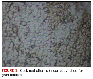
Many gold failures are incorrectly attributed to black pad issues.
Figure 1 shows the surface of a nickel pad on a printed board after stripping the gold from the nickel surface. The image shows limited evidence of corrosion on the nickel surface at the grain boundaries on a bare board. Some evidence of gold is also still visible. Solder joint failures when examined normally show far more corrosion around the nickel boundary. Much debate centers around the subject of black pad. Changes to nickel chemistry and better control have reduced solder joint failures.
Unfortunately, many gold failures are attributed to black pad issues, when clearly they are not. Close cooperation is necessary with the PCB supplier and its chemistry supplier to determine the cause of the problem. Always ask to review the chemistry supplier’s audit reports conducted at the PCB supplier’s offices. Independent analysis also may be required, if the assembly processes are considered the root cause of any joint failure. Review the PCB fabrication process, the reflow temperature and time in a liquid state for the solder paste.
These are typical defects shown in the National Physical Laboratory’s interactive assembly and soldering defects database. The database (http://defectsdatabase.npl.co.uk), available to all this publication’s readers, allows engineers to search and view countless defects and solutions, or to submit defects online.
Positioning CSPs and noise-sensitive devices are two of a host of considerations.
Effective, accurate component placement takes into account the best practices of design and assembly, both of them inextricably intertwined. The layout engineer must take special care to correctly place components on the board, since this has a direct bearing on assembly and testability.
Also, with the evolution of various technologies, assembly takes on newer meanings, dimensions, and demands. In particular, use of fine-pitch BGAs is escalating, challenging current assembly practices and procedures. In these situations, PCB design and assembly know-how and experience are the linchpins for effective placement.
Design for assembly takes into account such factors as through-hole versus surface mount components, critical ribbon and cable assemblies, cutouts, vias, decoupling capacitor placement, mechanical aspects, and others. Through-hole technology has become more of a specialty, while surface mount is the basis for most of today’s designs.
In terms of placement and routing, the beauty of an SMT design is its superior leverage relative to board’s real estate area, because both sides of a board can be utilized. This creates certain challenges, however. For instance, an experienced PCB designer doesn’t want to place a noise-generating device or high–frequency, sensitive device close to the clock where the signal will incur interference. Improper component placement raises the probability of high-level noise and an unacceptable signal-to-noise (SNR) ratio.
Through-hole mostly is used for connectors and mostly is limited to signals coming into and exiting the PCB. However, SMT connectors increasingly are used. But some applications employ a combination of surface mount and PTH components. When a PTH connector is used, another component cannot be placed on the other side of the board since there’s no usable real estate.
The advantage of a surface mount connector is both sides can be used for component placement. However, the PCB designer must take precautions when placing either PTH or SMT I/O components. The same concepts apply to other components with gold fingers, ribbons, or cables attached to the board. Usually, the physical location of these devices is fixed. For example, a gold finger of a daughtercard going into a motherboard needs to be at a certain location to ensure a proper fit. At the same time, the board designer must ensure space limitations are not violated and no mechanical, vibration, or height-related issues are created due to that particular placement.
The designer also must check that all X and Y coordinate calculations are accurate. This means the cutout or gold finger is made at the right location because if a hole is off by, say, 0.010˝ to 0.020˝, then a pre-selected cable will not go in the right place. Physical location and dimension calculations cannot be fudged if I/O components are to precisely communicate with fixed devices from other systems or subsystems to the PCB.
As for vias, there are an array of types, including blind, buried, stacked, and through-hole vias. A through-hole via goes from one side of the board to the other. Blind vias go from an outerlayer to a middle layer; for example, a blind via originates at the top layer and terminates at one of the innerlayers. Buried vias originate and terminate within innerlayers. Stacked vias originate from each of the outerlayers and terminate on the innerlayers at the identical location.
When it comes to selecting vias for accurate component placement, the designer must consider the pros and cons of each to avoid assembly issues later. For example, for smaller and handheld devices, which are compact in terms of available real estate, there is sometimes no choice but to use blind or buried vias. These particular vias are difficult to fabricate and increase manufacturing cost. The advantage of these vias is that routing and connections use the innerlayers, thereby saving top and bottom layers for component placement and critical routing.
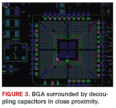
Signal integrity is another major DfA aspect when it comes to component placement. It is critical to appropriately place bypass capacitors next to BGAs, CSPs or QFNs. This is especially true in high-speed designs, for which transmit and receive paths must be highly accurate and extremely short, to avoid impedance control issues. The signal from a BGA ball to a bypass capacitor must be cleanly filtered to suppress noises, hence the importance of maintaining close proximity and placement of these capacitors next to BGA, CSPs and QFNs.
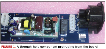
If the board has too many components close to the edge and protruding from the board (Figure 1), it’s best to use tab and route, versus scoring during board fabrication. By using tab and route, there is a small portion of rail to separate two boards from each other. On the other hand, a scoring device separates boards next to each other and is not ideally suited for boards with protruding devices.
Also, for efficient assembly involving small board sizes that are panelized, create accurate fixtures for handling PCBs during reflow soldering. But a panel must not be made too large; optimal panel size must be calculated to maximize manufacturing efficiencies. Otherwise, the board could warp from the component weight. Aside from proper assembly techniques, DfA compliance also deals with different tools and the point to deploy them during assembly. For instance, will x-ray be applied as a process check at the end of each board or for sampling one of every five, 10, or 20 boards? When will a certain fixture be used? During surface mount? Wave solder? Or maybe at AOI or testing? These issues need to be addressed at the planning stage, when the CAM engineering/planning department is reviewing the data and preparing the processes and visual aids for the jobs.
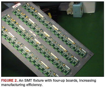
Not all machines will be able to use the same fixture, due to varying dimensions. But they will be different because they’re created to conform to different board sizes. Moreover, they have their own mechanical and tolerance limitations. Be aware of these tolerances, as a universal fixture is not a cure-all. At times, there must be multiple fixtures, one for SMT (Figure 2), another for wave solder, and still another for testing. Most often this occurs when boards are smaller and not uniform. For example, they may be semi-circular, round, half moon or L-shaped. In these cases, various types of fixtures are used to make assembly an easy, reliable and repeatable process.
As far as BGAs are concerned, they demand special scrutiny and attention. BGAs require just the right amount of solder paste. Too much could cause shorts between the balls. Then there’s no choice except to depopulate and re-ball it, or use a new BGA device. Moreover, it’s important to ensure correct placement, keeping in mind component orientations and polarities. When rework is involved, sometimes it is important to desolder the nearby decoupling capacitors (Figure 3) or other devices, making rework possible.
Also, BGAs should never be placed close to the board’s edge. Reason: A BGA needs a peripheral area that’s heated during rework. If close to the edge, then that half side close to the edge will not sufficiently heat, simply because there’s no mass around the BGA device to heat. Hence, the BGA will be extremely difficult to depopulate.
At the stencil design stage, sound assembly practices depend on the decisions over foil thickness, stencil frames, aperture to pad ratio, for dispensing correct amounts of solder paste, when to use window panes, performing first article inspection, and the right type of solder paste, along with use of paste height measurement systems.
Foil thickness determines the amount of paste to be dispensed. Assembly personnel must determine whether a stencil will be 0.04˝, 0.06˝ or 0.08˝ thick to gauge the amount of paste required. As foil thickness changes, it changes the amount of paste dispensed on pads, thereby affecting the thermal profile. Foil should come framed from a vendor. Stencil foils without frames create time and reliability issues. Time-consuming mistakes may include mounting the foil upside down or in reverse, and damaging it. Also, when stencil foils are not stretched properly when mounted on the adapter, it can adversely affect the quality of the paste deposit, causing bridging and misregistration on the SMT pads.
Aperture-to-pad ratio decisions, for example, can be whether those ratios will be 1:1, 1.1:1 or 0.9:1. The ratio 1:1 means size of the stencil opening is equal to the SMT pad. A 0.9:1 ratio means the size of the stencil opening is smaller than the SMT pad, thereby dispensing smaller amounts of paste. This mostly is used in ultra-fine-pitch SMT applications.
Sometimes a stencil opening is made a bit larger compared to the pad size so that the aperture to pad ratio becomes 1.1:1. This permits slightly more paste to be dispensed on the stencil. This is mostly used in heavy analog applications. In each case, assembly personnel must be fully aware of a board’s end application and whether the dispensed solder paste is adequate. Some studies have found as much as 75% of defects are related to paste dispensing, which bears directly on stencil design.
Window panes are implemented when there is a huge opening on a stencil design. Consider a 0.5˝ x 0.25˝ opening, which is extremely large when it comes to dispensing paste. Therefore, a decision is made to pane the window to create smaller window or opening sizes within the large opening. For example, six different slots or panes may be created to control the amount of paste going to these different panes versus applying a whole blob of paste on the pad.
Also, every time a decision is made involving stencil design, it’s vital to perform a first-article check to ensure the proper amount of paste is dispensed, or whether another foil needs to be cut due to a thickness or aperture-to-pad ratio change. This would act as a process verification tool for dispensing the right amount of paste on the pads.
Here’s where a first-article inspection system proves invaluable. FAI systems are relatively new. They help create the first-article board by scanning the image of the whole board (the golden board), and comparing the images of all other boards with this golden board to ensure all components are placed properly, with correct orientation and polarities. It is used as a process verification and inspection tool to significantly reduce the human interface and make inspection and QC more reliable, repeatable, and faster by at least 30 to 50%.
Last, solder paste and its varieties are vital considerations for accurate component placement. Normally, Type 2 and 3 solder pastes are used for analog devices and analog/digital. Sometimes Type 4 (or finer) is required for fine-pitch BGAs, CSPs, and QFNs.
Generally speaking, solder paste is a mix of metal grains and certain chemicals in a format conducive for soldering. Those metals are of considerably finer grain in Type 4 compared to Type 3. This means Type 4 can be used more accurately for fine-pitch components because its tolerance is slightly higher compared to Types 2 and 3. Viscosity for Type 4 is finer. This means grain particles are joined tighter together compared to those of Type 3, and thus can be used more accurately for fine-pitch components.
Fredrick Grover’s invaluable tome is essential for partial inductance calculations.
Inductance is probably the most confusing topic in signal integrity, yet one of the most important. It plays a significant role in reflection noise, ground bounce, PDN noise and EMI. Fortunately, the definitive book on inductance, originally published in 1946 by Fredrick Grover, is available again.
After two printings in the 1940s, Grover’s Inductance Calculations was out of print by the mid 1980s. It was just reprinted this year and is available from Amazon in paperback (amazon.com/Inductance-Calculations-Dover-Books-Engineering/dp/0486474402/ref=sr_1_1?ie=UTF8&s=books&qid=1260191720&sr=8-1) for a very low price.
Motors, generators and RF components experienced a period of high growth in the 1940s. At their core were inductors, and being able to calculate their self- and mutual-inductance using pencil and paper was critical. (Keep in mind this predated the use of electronic calculators.) While many coil geometries had empirical formulas specific to their special conditions, Grover took on the task of developing a framework of calculations that could be applied to all general shapes and sizes of coils.
While Grover does not explicitly use the term, what he calculates in his book are really partial inductances, rather than loop inductances. A raging debate in the industry today is about the value of this concept. Proponents say it dramatically simplifies solving real-world problems and is perfectly valid as a mathematical construct. You just have to be careful translating partial inductances into loop inductances when applying the concept to calculate induced voltages. Opponents say there is no such thing as partial inductance; it’s all about loop inductance, and if you can’t measure it, you should not use the concept. There is too much danger of misapplying the term.
I personally am a big fan of partial inductance, and use it extensively in my book, Signal and Power Integrity – Simplified. It eases understanding the concepts of inductance, and highlights the three physical design terms that reduce the loop inductance of a signal-return path: wider conductors, shorter conductors, and bringing the signal and return conductors closer together. Most important, partial inductance is a powerful concept to aid in calculating inductance for arbitrary shaped conductors.
Inductance is fundamentally the number of rings of magnetic field lines around a conductor, per amp of current through it. In this respect, it is a measure of the efficiency for which a conductor will generate rings of magnetic field lines. To calculate the inductance of a conductor, it is a matter of counting the number of rings of field lines and dividing this by the current through the conductor. Counting all the rings surrounding a conductor is really performing an integral of the magnetic field density on one side of the conductor.
Literally everything about the electrical effects of interconnects stems from Maxwell’s equations. Grover starts from the basic Biot-Savart Law, which comes from Ampere’s Law and Gauss’s Law, each, one of Maxwell’s equations, and derives all his approximations. The Biot-Savart Law describes the magnetic field at a point in space from a tiny current element.
Using this approach, Grover is able to calculate the magnetic field distribution around a wide variety of conductor geometries and integrate the field (count the field lines) to get the total number of rings per amp of current. Using clever techniques of calculus, he is able to derive analytical approximations for many of these geometries.
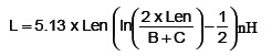
The most commonly used approximation is for the partial self-inductance of a long, straight rectangular conductor, such as a lead frame in a QFN package or a connector pin. He calculates it as:
where L = the partial self-inductance in nH B, C are the thickness and width of the conductor cross section in inches Len = the length of the conductor in inches.
For example, for a 1˝ long lead, 0.003˝ thick and 0.010˝ wide, the partial self-inductance is 23 nH. This is roughly 25 nH per inch, or 1 nH/mm, which is a common rule of thumb for the partial self-inductance of a wire.
If you deal with connectors, packages, vias, board discontinuities or odd-shaped transmission lines, and need to estimate the loop inductances of non-uniform sections, Grover’s book is a great resource. You will have a great collection of inductance approximations at your fingertips. It is well worth the low price.
Dr. Eric Bogatin is a signal integrity evangelist with Bogatin Enterprises, and has authored six books on signal integrity and interconnect design, including Signal and Power Integrity – Simplified, published in 2009.
Offshoring works best for stable designs and predictable demand.
“We need to try to bring the price down some more,” the customer told me over the phone.
It was 2005 and the company I worked for was a custom OEM primarily serving the telecommunications industry. After the telecom collapse, everyone wanted the lowest cost possible, and no one was able to forecast sales beyond three months. Long-term purchase orders that helped with downstream planning were a thing of the past. We already had squeezed the supply chain as much as we could; without longer-term planning, I was unable to get additional volume discounts on material. The customer was a startup, though, and was attempting to hit a price point that it was sure would sell decent volume. We were looking at around 2,000 pieces per year, which for us was high volume.
After management review, we decided to attempt to outsource the board for cost savings. I had some experience with Chinese manufacturing, and our company was in the process of setting up an office in India with an eye toward offshoring certain engineering operations and assembly. The thinking was, by having our own office in a low-cost country, we would be able to better manage the offshore suppliers. I sent RFQs to China and to our Indian office. Even at the lower volume, I was able to find cost savings: 35% in China and 25% in India. For various reasons, the Indian supplier was selected, and the customer was happy with the cost savings. Now it fell to me to manage the supplier.
I had heard the horror stories associated with offshore sourcing, mostly related to product quality. I had one customer that set up a closed-circuit camera in one of its offshore partners’ facilities. When boards were completed, the manufacturer (in India) placed the finished product on a table under the camera. The US customer logged into the camera and inspected the boards remotely before permitting shipments. This situation seemed overly involved to me, and was one I was determined to avoid. Worldwide shipping services had largely eliminated cost concerns I had previously heard about in early offshoring discussions. I no longer needed to wait for a container to be full to get product shipped at an acceptable cost. Sure, it was more expensive than my local supplier delivering the boards, but that cost adder had been factored in my sell price to my customer. I also had been warned of language barriers and time zone delays as potential issues. I found the majority of my contacts in India spoke English nearly as well as I did – accented English, to be sure, but still very understandable. The Indian companies we did business with had also set their mid- and upper-level management personnel on second shift. This allowed them to work with our normal first-shift hours in the Eastern time zone. We also had local representatives who could be sent to the manufacturing facility to oversee our needs.
Initially, the relationship worked rather well, despite my reservations and fears. As time elapsed, however, we began to run into issues, primarily with on-time delivery. The supplier was unable to efficiently adjust to our needs, based on either material availability in country, or assembly capacity. We needed releases of 200 pieces, but they would run 500 at a time. Units would fail test, and instead of asking for help troubleshooting, they would push them aside in favor of other customer demands. We’d make engineering changes, and they would neglect to update their assembly documentation, or make us take previous revision boards due to their overruns. We had never discussed minimum lot quantities, nor were they a condition of the contract. The supplier also purchased material at much higher quantities than needed for the orders we had placed, and then asked us to cover the material overage costs, another item that was not a condition of its quote, the contract or our purchase order.
Most issues we encountered were similar to issues encountered with local suppliers, but were aggravated by the distance. I was unable to effectively manage the issues with the time zones involved while maintaining adequate lead times. The stateside overhead required to manage the product was not factored into a landed cost analysis of the product, and quickly absorbed any cost savings. In the end, we were forced to bring the product back onshore so that it could be efficiently produced and managed.
As with all outsource evolutions, planning is essential to successful offshoring. If the design is not stable, or demand not relatively predictable, the odds of success decrease. Stateside management costs must be factored into the landed costs, more so with volatile demand products. I believe offshoring could be an effective solution for the right product and volume mix. However, offshoring is not a viable option when demand is variable and the design is not stable. Stick with a flexible onshore supplier for these sorts of products.