OEMs are no longer leaving test strategies in their supply-chains’ hands.
In my role as a technical marketing engineer, I work with test engineers from OEMs, EMS companies and ODMs, learning about their test needs and challenges, which range from common threads to unique needs. One industry commonality is the continuous need to drive down the cost of test. This may be obvious, especially during the recent economic downturn, but even when the market is buoyant, manufacturers continue to expect us to lower test costs, while expecting far greater coverage and test capabilities. When you drill down a little further though, the differences in expectations start to emerge.
While OEMs have traditionally been pioneers when it comes to technology adoption, I have observed that for EMS firms and ODMs, new test technology is a need rather than a choice. While EMS companies do play in the consumer electronics market, many of the bigger players also manufacture more sophisticated products like high-end server, datacom and telecom boards – products that do not face the harsh cost pressure of consumer electronics. There are still cost-down expectations for these products, of course, but EMS firms traditionally have been more willing to invest in newer test technology to overcome the challenge in testing assemblies with technologies such as high-speed differential signals.
That’s not to suggest ODMs are not investing. OEMs are driving their ODM supply chains to adopt new technology to keep up with product requirements such as notebook motherboards with high-speed differential signals, and to cope with PCB real estate demands as the number of nodes increase while the PCB size decreases, making it harder to put testpoints on the board.
We see our key EMS customers involved with manufacturing high-end boards ranging from 7,000 to 10,000 nodes for, say, high-end servers; these are very expensive products, and manufacturers will do everything to achieve maximum test coverage, employing a blend of x-ray to in-circuit and sophisticated functional tests. For ODMs, cost and time-to-market are more pressing issues. While maintaining higher test coverage requirements, ODMs also demand faster test methodologies at even lower costs, with their investments typically centered on a combination of manufacturing defect analyzers, in-circuit tests and functional tests at the board level.
It was observed some years back that OEMs were leaving test strategies more in the hands of their outsource partners. However, I think that trend has petered out, as the pace of technology development puts pressure back on OEMs to drive contractors toward higher standards of tests, to cater for wider and more in-depth test coverage for the onslaught of sophisticated components.
Concurrently, the proactive role played by many OEMs within industry bodies such as IEEE, iNEMI and other initiatives to drive new standards on boundary scan and BIST tests, just to name a couple, will help speed technology adoption.
Within the industry, the role of the outsourced service providers or vendors will grow in depth compared with a few years back. The reason for this is the level of engineering responsibility within the larger manufacturing organizations is rapidly evolving. Many of my production engineer contacts are no longer just engaged in test engineering roles: They wear multiple hats, which include coordinating requirements with customers, managing yield, managing system maintenance, and working with test system application engineers, as well as test program and fixture vendors.
Production engineers no longer have the luxury of time to work on deeper-level debugging and test development. However, another new equilibrium is taking shape, with the workload flowing to more test solution providers and fixture vendors – themselves a growing new breed of technopreneurs, if I may leverage this term to describe engineers-turned-small business owners who still operate within their domain knowledge.
The fallout from the recent economic downturn created new opportunities. In China, there is a well-known term for this called wei ji. The phrase means “crisis,” but the individual characters stand for “danger” and “opportunity.” Many of the technopreneurs who lost jobs during the downturn now find themselves fitting a timely and niche market to provide services back into the supply chain from which they came, albeit now with more flexibility and scalability.
For test equipment vendors to be successful, they need a solid network of partners, and technopreneurs help expand and strengthen that network by providing the needed technical knowledge in test development and debugging, as well as cost-effective local responsiveness required in the 24/7 manufacturing environment.
Test equipment vendors also have a growing responsibility – as technology coach and innovator. Not only must vendors continue to innovate in test, but we also must train our internal team well, which consists of the entire network of expert application engineers, field sales engineers and support partners – from fixture vendors to application solutions providers, certainly not forgetting the end-customers, to ensure they are technology-ready. In this respect, one common challenge across the industry is resistance to change whenever a technology is introduced. The groans of many production engineers are almost audible when we try to introduce a technology on top of already numerous responsibilities. Moving forward, training will grow in importance to ensure each area of this EMS-ODM-CEM equilibrium can evolve rapidly to adapt not just to new technology, but to the shorter, sharper economic cycles we have come to expect.
Jun Balangue is technical marketing engineer at Agilent Technologies (agilent.com); This email address is being protected from spambots. You need JavaScript enabled to view it..
Fall was the season of mergers and acquisitions: Viasystems and Merix; TTM and Meadville; DDi and Coretec. Likewise, you hold in your hands a merged product – PCD&F and Circuits Assembly. Like many of the industry deals, this was borne both of necessity and opportunity. The good news is, with our stable of editors, including Pete Waddell (20 years of design work), Kathy Nargi-Toth (a similar amount on the fabrication side), and my own 18-plus years covering design, fabrication and assembly, we have the technical chops and experience necessary to make sense of the fast-moving electronics manufacturing world. Going forward, our two brands will retain their identities, including their own websites. Meanwhile, the printed magazine – the last remaining monthly publication in North America covering electronics manufacturing – gets a boost in size and circulation. Win-win.
I have mixed feelings about DDi’s pickup of Coretec. On one hand, Coretec was finding it extremely difficult making it as a small yet publicly held company. Its sales had slipped from C$92 million in 2006 to C$81.4 million in 2008 – an 11.5% drop – and were on a run rate of $72.7 million this year. Worse, it was still seeing sequential declines through the September quarter, while competitor DDi has begun the upward revenue climb. Its last quarterly net profit was the fourth quarter 2006. And with no cash on hand, its hands were severely tied. All of which might explain why Coretec’s CFO position has been something of a revolving door for years.
DDI, on the other hand, has turned the corner after years of questionable acquisitions, two bankruptcies, and a notorious internal culture. It’s turned a profit all three quarters this year. That said, DDi has just $25 million in cash itself, and PWB fabrication is a cash-intensive business, with lots of ugly cycles. While I suspect DDi saw an opportunity to beat some competitors to the punch by bidding on Coretec now, I can’t help but think that had they waited, they might have picked up the company more cheaply. And I’d hate to see several years of work undone by a deal gone bad.
Meanwhile, TTM’s purchase of Hong Kong-based Meadville’s board business opens a huge can of worms, as it would put the father of Hong Kong Chief Secretary for Administration Henry Tang in position to own 33% of TTM. But knowing a little about how government works, even when a Chinese government official is the offspring of the biggest shareholder of the leading bare board supplier to the US Department of Defense, it says here the real stunner would be if US anti-trust regulators saw a potential conflict and nixed the pending deal.
Warming in Munich. November’s biennial behemoth known as Productronica was, all in all, a better-than-expected show, modest by historical standards, but strong compared to everything else this year. Perhaps more important, after a year of malaise, there was a noticeable improvement in the general outlook for 2010. Almost across the board, the more than 80 companies we spoke with during the show see 2010 already emerging as a brighter year. The strong consensus is that the worst is past, and while there remain certain structural problems – including major banks’ inability or refusal to reopen credit lines – business is picking up in most sectors, led – perhaps surprisingly – by automotive.
Much like the two major China shows and Apex, Productronica this year was dominated – capital D – by regional visitors. And I am coming to believe the ongoing regionalization has less to do with the economy and more to do with the fact that for the very most part, existing production technology can build even the latest and greatest products. No matter that new generations of end-products come out every six months (or less), processes are driven by component packaging, and while leading-edge package types have shrunk from 0402 to 0201 to 01005 during the past five years, most conventional equipment is so darn good that it can print, place, solder, inspect and test the latest package styles. Assemblers simply no longer need to chase the latest and greatest equipment around the globe to win or build the latest designs. And that, in turn, obviates the need to run from show to show in search of the “next big thing.”
Year ends. KeyTronicEMS is one assembler that never has been the “next big thing,” but based on a six-year track record of net profits, it clearly should be in the conversation. Be sure to check our profile of the Circuits Assembly EMS Company of the Year this month.
2010 will bring our third annual Virtual PCB trade show and conference. This year promises to be the best yet. Click on www.virtual-pcb.com to learn more.
Our sincere hope that all our readers have a healthy, happy 2010!
A look back at friends and colleagues who left us in 2009.
2009 came in like a bear and left like a lamb, but was felt deeply by all. Likewise, many of our friends and industry colleagues who did not make it through the year leave behind remarkable legacies and compelling memories. This month we reflect on their impact on our industry and our lives.
Dr. Carl Tautscher, 83, cleaning expert, author, and chairman of the IPC Cleaning and Contamination Control Subcommittee.
Jim Thiel, 61, cofounded Thiel Audio.
Richard (Dick) Schedtler, 60, vice president and owner of AR Marketing, and former Intel engineer.
Marty Jawitz, 78, former Litton Guidance and Controls engineer and author.
Velma J. “Val” Greig, 71, former auditor at Tektronix and Merix.
Dr. Steven Case, 60, founder and chairman of CyberOptics Corp.
Jerry Lee Cartwright, 51, engineer at Western Digital and Celestica.
Barry O’Brien, 56, late of Horizon Sales manufacturer’s representative, MidWest Circuit Products and Foundation Technologies.
Bradley Jay Black, 50, ex IBM, Celestica, and Ayrshire Electronics.
James (Jim) J. Miller, 76, product development engineer, Laminating Company of America (LCOA), BF Goodrich and Daubert Chemical.
Roy Matheson, 83, former production engineer at Sheldahl.
Scott Hudson, 52, semiconductor industry analyst at Dataquest, In-Stat, IDC and iSuppli Corp., and former staffer at Apple and Sanmina-SCI.
Allan McKinnon, founder, rep company Allan McKinnon & Associates, and PCB wet process equipment manufacturer FSI.
Harvey Simonds, 48, former field service engineer at Vitronics-Soltec and service technician at Xerox.
Mark Shepherd Jr., 86, 40-year veteran in engineering and management Texas Instruments; was chief executive from 1967 to 1976 and chairman from 1976 to 1988.
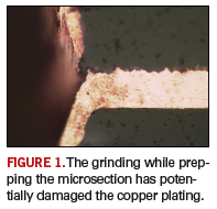
Microsectioning shouldn’t be taken lightly, lest the sample be damaged.
The microsection image shows an open connection between the through-hole copper plating and the innerlayer tracking. The microsection has been poorly prepared, with potential damage to the plating during grinding. As shown, no resin is in the hole to support the through-hole copper plating. The surface of the copper is rounded, making it impossible to prove the root cause of the problem in this example.
It is accepted that the sample has been poorly prepared. Any time a section is being prepared, it is important resin enters the through-hole. In the case of via holes, they may be coated with solder mask; in this case, the mask surface must be broken to permit resin to enter the hole. If a section is found to not have resin in it prior to grinding to the center, it’s important to stop grinding. This permits the hole to be filled with resin, recurred prior to further grinding of the sample.
These are typical defects shown in the National Physical Laboratory’s interactive assembly and soldering defects database. The database (http://defectsdatabase.npl.co.uk), available to all Circuits Assembly readers, allows engineers to search and view countless defects and solutions, or to submit defects online.
Dr. Davide Di Maio is with the National Physical Laboratory Industry and Innovation division (npl.co.uk); This email address is being protected from spambots. You need JavaScript enabled to view it..
For most, the road forward centers on offering the lowest cost product, or providing exceptional and/or unique service, or being at the cutting edge of technological innovation. Most would probably agree the migration toward Asia originated with, and has prospered from, the pursuit of the low-cost business model. Exceptional service is ever evolving and often specific to end-market or geographically driven needs. Companies the globe over tailor their unique interpretation of service to the needs of targeted customers and markets. Many believe technological innovation, the backbone of our “high-tech” industry, to be the last bastion of strength for (higher-cost) Western companies. Offering cutting-, if not bleeding-, edge technology for demanding, R&D-focused OEM engineers working on the next-generation “wow” is continually mentioned as the hallmark of the remaining Western companies.
The problem is, maybe that paradigm is shifting.
Much has been said and written about the evolving electronics industry, its migration, and the cost drivers that have left as carnage once big-name and proud industry pioneers. What has emerged from those ashes are smaller, more technically “niche” focused companies that are lean and mean (read: minimally staffed) and evolving process and technical advancements (read: do it on the fly). These smaller companies think about intellectual property more as something linked to software they use rather than their expertise in providing product. Equally, technological advances are often, but not always, gauged via the rearview mirror of what it took to get an order out, rather than what might lie ahead if that new technology is applied to new applications.
What goes unacknowledged is where technology is being developed and with whose IP. Technology development is made public in several ways. Sometimes it takes the form of white papers presented at technology associations. Sometimes dramatic press releases reveal the latest, greatest product and refer to the IP developed to make it happen. Another, more easily understood method is to track the number of patents issued – in particular US patents. In this sense, the number of US patents issued related to printed circuit boards rapidly is being controlled by non-American companies. In particular, measured by patent applications, Chinese companies seem to be more technologically innovative and IP-creating than all North American companies combined!
What does this mean? One observation is that maybe some of the smaller companies – companies historically not staffed with R&D departments, not known for generating IP, and less worldly about the process of protecting the same – are now the de facto drivers of technological innovation. The message for all companies – large OEMs to circuit board fabricators to small design bureaus – is that with the demise of some of the larger R&D-driven fabricators, the offloading of PWB R&D by major OEMs to suppliers, and the need for everyone to become more focused on technology vs. just offering “me-too” capacity, the paradigm is shifting as to who and how technology may be developed. Smaller companies need to better understand IP and large companies need to better understand the emerging new supply base.
Understanding IP is very different from developing new technology. Designers understand well the importance of their ability to create IP. Fabricators, on the other hand, don’t. Most fabricators work on getting the job done – developing processes and capability to satisfy the immediate order – and don’t fully understand that those efforts are their IP. Many of those efforts are cutting edge and very patentable. All efforts to develop technology must be looked at equally as IP – not just the pain and suffering expended satisfying an order.
For smaller companies without formalized R&D initiatives, how they satisfy customer requirements needs to be reconsidered. Documentation needs to be developed to capture what is done, why, and with what end-result in a way that explains the R&D that went into creating the IP that led to higher technology. Any run-and-gun environment hates slowing to commit pen to paper, but the rewards can be huge. Short-term, R&D credits are available.
Longer-term, the technology library is created so technologically savvy customers can see your company has the ability to provide value-add R&D to assist their ascendency. And finally, out of some efforts may be patentable, groundbreaking technology that profoundly differentiates your company from the pack. This may be the greatest opportunity: creating long-term value by applying what you already do to a more formal R&D process that yields global recognition in the form of patents.
For larger companies, the shift is to embrace smaller companies that offer needed unique niche technology, and are in the best position to further develop that technology. This requires much more active involvement and commitment to working with a greater number of companies, many of smaller size. The benefits, besides attaining the desired technological development, are to broaden the supplier base with companies that are equally committed to an OEM’s technological needs and servicing that company as a valued customer. Larger companies may find there are more committed suppliers in their backyard than they thought, and those companies are best able to satisfy technological development.
For all companies, the need to understand technology and IP needs revisiting. How technology is approached – how we view IP – will determine who in the future is in a leadership position. Our industry is once again at a fork in the road. Following the route focused on rethinking IP may well be the best path forward.
Peter Bigelow is president and CEO of IMI (imipcb.com); This email address is being protected from spambots. You need JavaScript enabled to view it.. His column runs monthly.
Designers’ fight for proper recognition has lasted 20 years.
The question was a familiar one. “Pete, what can we do to raise the visibility of designers and acknowledge the role they play in product development?”
A marketing guru at one of the major PCB EDA companies asked me this. It sounded familiar because it is the same question I asked 20 years ago when I first went to work for Printed Circuit Design magazine. Fresh off a design job, I had been hired as the green editor with a new cause and a head full of ideas about what the magazine could do to focus on PCB design and designers.
Not long after, I met some folks who were trying to start a global organization for designers. Within a short time, the IPC got involved, and thanks to Gary Ferrari and Dieter Bergman, among others, the IPC Designers Council was born. The excitement was palpable. Soon, local chapters were springing up all over the world. Printed Circuit Design ran ads in the magazine and did mailings to our subscriber list to encourage participation. When time allowed, I attended meetings all across North America. Even my home chapter in Atlanta had around 50 members, and 30 to 40 designers and engineers regularly attended monthly meetings.
Looking for the glue that would hold the organization together, and a feather designers could put in their caps, the organization developed the Certified Interconnect Designer program. The CID program was intended to certify a designer’s core competencies in design based on IPC standards.
Many designers signed up and took the basic certification test, and the Council directors moved to add more modules to the program based on advanced technologies and techniques. Gary and Dieter were very involved in the effort, and poured their time and energy into the Council with gusto. For a time, all was right with the world. The council grew, and before long, there were close to 50 local chapters in North America and Europe holding regular meetings.
Then slowly, but perhaps inevitably, the air went out of the balloon. Attendance fell and chapters began to go inactive. Today the IPC lists 23 local chapters. I recently sent emails to the email addresses of all 23 chapter heads, asking whether the chapter was still functioning and what activities they had planned. I received answers from nine, although I know that at least two or three more remain active. Five said they had regular meetings, and the other four described their chapters as active, but in their words, “on life support.” (Funny how all four used the same words.)
What happened to the excitement? What about all the hard work the local folks put into building the organization and the dreams of an active, global organization for PCB designers? Apathy, workload and lack of leadership are the comments I hear most. Many local chapter officers served several consecutive terms and grew tired of handling the load. Some said that they had trouble finding speakers for the meetings, or felt there was no compelling message or reason for attending.
On the positive side, several chapters are very active. North Carolina holds a conference and trade show every year and has been very successful. The Austin (Texas) chapter holds a Vendor Night every August. But, even if all 23 chapters were active, it would not be a ground swell.
Getting back to the original question, I’m not sure what we can do. Let’s estimate an average 50 members for each chapter. With 23 chapters, that’s 1,150 members. No one has hard numbers on the size of the PCB designer community. At one time we estimated there were 100,000 designers and engineers involved in PCB design in North America alone. Even if the number were half that today (it’s probably more), then Designer Council membership would be 2% of the audience. Maybe that is a good number, but it does not sound that good to me.
Editor-in-chief Mike Buetow has come up with a couple ideas that we plan to use in the coming months to highlight significant contributions designers have made to a project. We’re also looking for ideas from you. Whether you are involved in design or fab, we want to hear what you think PCD&F can do to increase the visibility of designers and acknowledge the role they play in product development. Email me at This email address is being protected from spambots. You need JavaScript enabled to view it. or go to our blog at pcdandf.blogspot.com and make yourself heard.
Pete Waddell is publisher and design technical editor of Printed Circuit Design & Fab/Circuits Assembly; This email address is being protected from spambots. You need JavaScript enabled to view it..