
Determining your optimum geometry, plus two methods for providing data to the fabricator.
Controlling impedance (resistance) is almost a given with today’s technology. One day we are adding a wireless option to a common object and calling it the Internet of Things. The next day we’re simply keeping up with the competition on processing the code. The trend is toward a greater percentage of the connections falling under the domain of impedance control.
Controlled impedance has two main branches: Single-ended transmission lines are the backbone of RF technology, while differential pairs do the heavy lifting for digital circuits. We’ll start with the single-ended lines. They have a start and an end point. The signal is sent one way on the transmission line, and the circuit is completed over the adjacent ground plane.
The main factor influencing impedance is the width of the trace relative to the thickness of the dielectric material between the trace and the ground plane – or planes – used as a reference. What is a reference? It is usually a metal plane with zero volts – “ground” but can have a few volts of its own, either positive or negative relative to what’s happening on the trace itself.
A mixed-signal board is always a stretch, with the various functions vying for limited space.
A basic rule of thumb is the width of the trace is nearly equal to the thickness of the dielectric material to achieve a 50Ω impedance on the line. The exact number is a product of a number of factors that define the optimum trace width.
Two primary factors determining the trace geometry are the thickness of the copper and the dielectric constant of the material (Dk or Ɛr). Exotic materials are known for their thermal stability, their tight control over the dk and for a low-loss tangent. Those properties come at a cost. The ceramic materials are typically found in high-frequency and very high-speed applications. Good design practices with FR-4 usually do the trick.
Additional PCB layers above the trace have an impact, as they require a transition between stripline and microstrip geometry. On balance, the line is normally thinner on the innerlayers, but you’re compelled to provide a continuous ground plane on the layer above and below the innerlayer transmission lines.
The presence of solder mask can affect routing on the outer layers to some degree. Any kind of coating or large ferrous metal objects can affect an analog signal. The final line width and construction adjust for those factors.
Differential pairs in the real world. Turning to the digital logic side, our favorite way to spew ones and zeros is to calculate the difference between two matching lines, rather than trying to read a single line that is subject to momentary instances of noise as a voltage spikes across the landscape.
The noted dimensions create the space for the digital waveforms to propagate. The stuff between the metal is the medium whose properties determine the rest of the values. (Source: Maxfield EEWeb)
This is how differential pairs are different. Too much can go wrong with a long enough transmission line, and dropped packets are followed by check-sum bytes that do not add up to the number of bytes actually received. Whatever those instructions were, they must be repeated. The user gets beachballs, hourglasses or, heaven forbid, stalled video!
A good microphone cord has the triple connection, so it doesn’t pick up so much noise from the alternating current fields that flow around wherever they will. My guitar hits with a stronger signal, so the two-wire cord is fine. That’s pretty much the two essential methods of data transport.
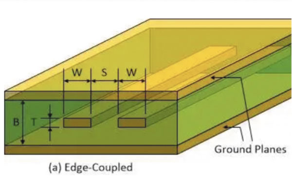
This plays out on the PCB as well. The second line, along with the ground, forms a balanced circuit. We can use a low voltage and still transmit good data over a fair distance. The common approach is to use edge-coupled lines. They are routed side by side, and the gap between them is a major variable. Loosely coupled lines are noted by the spacing between them being wider than the traces. Conversely, tightly coupled differential pairs have an airgap that is less than the trace width.
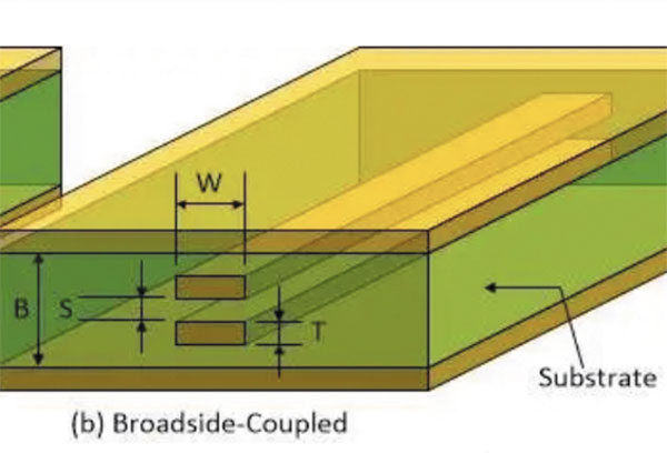
Stacking the traces calls for a tight layer-to-layer registration requirement. Missing by 25µm on a 100µm trace throws off the alignment 25%. (Source: Maxfield EEWeb)
So, after determining the optimum geometry for your purpose, it’s the fabricator’s job to carry this out. They have material and equipment that is hopefully aligned with your goals. Otherwise, keep shopping. Giving the PCB fabricator the data can take one of two forms.
Method 1: Provide a target and let the vendor come up with a plan. First and most common is to have a set of instructions or a table on the fabrication drawing describing the target impedance of traces broken down layer by layer for each impedance type in use. Provide the line width and spacing where applicable, as well as the reference layer(s) for calculating the impedance based on specific materials and processes.
The note/table often reflects what is embedded in the PCB design software as the design rules. It’s common to have a callout for every type on any controlled impedance layer designated in the constraints to fill in the blanks.
The board may or may not have used every kind of trace on every available layer. If you cross out the subset of design rules not in use, it’s one question they don’t have to ask at tape-out time. Target the information they need by obscuring what is not in play if your flow uses a standard template for impedance.
Method 2: Provide an unwavering set of conditions. The other way is a little more authoritarian in that it establishes an exact type of material through slash sheets and listing other criteria deemed necessary. Then, there is no negotiation on the impedance control, only on the timeline and price for obtaining the material that meets the specifications.
This model served us well at a certain fabless chipmaker where we could not be sure every type of material was suitable for the demands of Snapdragon chips. When a PCB is sent out for fabrication, the vendor may want to reduce the amount of copper in the via or somehow cut corners. We had data! There were exactly the right number of vias and copper width to get the job done as designed. More than enough would make the chipset bigger. Marketing sets that boundary. It’s our job to make it work. We thus required a solid representation of the data, rather than using it as a jumping off point. The words “or equivalent” were strictly enforced.
A good number of vendors are still out there; it’s beneficial to keep your options open. If you have a solid relationship with a vendor, they will be able to generate a proposed stackup that meets your needs. That information is applicable to that vendor at that time. Not much else is guaranteed in this business. Whether you design to their spec or keep using the same rules as always is your business.
John Burkhert Jr. is a career PCB designer experienced in military, telecom, consumer hardware and, lately, the automotive industry. Originally, he was an RF specialist but is compelled to flip the bit now and then to fill the need for high-speed digital design. He enjoys playing bass and racing bikes when he's not writing about or performing PCB layout. His column is produced by Cadence Design Systems and runs monthly.


