
Keeping some margin on the table increases the chances of immediate success and leaves a little bit for later.
There are many more ways to constrain a PCB layout than when I started my journey as a semi-intelligent designer. Guardrails were put in place to smooth transition into fabrication once the layout is completed. The other thrust of newer rules concerns the shrinking timing budget of our digital interfaces, particularly the memory banks.
We have so many aspects we can control that it can be tempting to disable or ignore some of them. That is a completely rational choice to make. New features take time to learn and implement. It may not be so easy to get everyone on board for a new feature or a whole new iteration of the software.
I remember getting buy-in to move up to a different whole number revision of the ECAD tools by reminding the team we didn’t have to use any of the new features and could go on using the tool exactly as before. It’s easy to get comfortable with what you have if that gets the job done to everyone’s satisfaction.
What we do is observed by many of the people around us. A narrow focus ends with the various EEs and your management team. Truly satisfying everyone takes a much wider view of the situation. Who is watching? Practically the whole company – and then some.
We also serve the document control group with cohesive data in terms of names and descriptions that match what is established by the system. Purchasing has to bear the brunt of the flurry of technical questions when our documentation or design work is not up to standards. The PCB fabricator’s CAM team has to create the phototools from the geometry we provide. What they may have to do in the name of global micro-editing might surprise you. The manufacturing engineers have to automate the process of attaching and soldering the components to the board with a high yield. The test team has to bring up and debug the prototypes while working out a test plan for mass production. In final assembly, or second-op, hands are laid upon the completed board, and it is installed wherever it may have to go. Regulatory, quality, reliability, sales, marketing and other technical and non-technical groups depend on our skillful use of tools we have been given to do our jobs. Last on the list but first in priority, the true owners of the design are our end-customers.
All these people, along with the company’s shareholders, have a stake in what we do every day. Someone approved the purchase of these CAD tools based on the promise that it would enable a smooth evolution from concept to fully realized product. These end-to-end solutions are typically tied to whatever the chip team uses for the silicon, if you happen to be part of a company that has its own chipset. The onus is on us to make the most of the tools with which we are provided to make that vision come true. To do that, we have to get inside the PCB factory and analyze how materials flow through and are combined in the process.
The imperfections of layering: The cake is a lie! One of the first things to consider is layer-to-layer misregistration. No factory can consistently replicate what we have on our screens. If it could, we would not need a capture pad on the via. The drill and all the artwork would lay up perfectly, and that is not the case. The drill does not hit the exact spot over and over, and every layer of the board varies in its precise location (registration) with respect to the others.
Unless the PCB is Class III, it is designed to permit the drill enough positional leeway to miss the center of the pad by enough that it winds up with 25% of the hole outside of the copper area. Even if every layer has that kind of breakout in a different direction, that is still an acceptable board according to IPC standards for Class II PCBs.
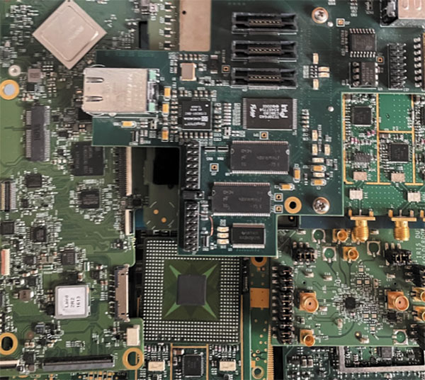
Figure 1. PCBs of all shapes and sizes have room for improvement.
An industry standard via hole is 8 mils (0.2mm) with an 18-mil pad. That’s plus five-thousandths all the way around in a perfect world. First, we consider the drill tolerance, and note it has to start out larger than the finished hole because the fabricator has to add a minimum amount of plating to the barrel of the via. That plating takes up one of the 5 mils we have to play with.
Account for drill size (+0.003/-0.018) and location accuracy (+/-0.003) over layers of naturally mis-registered artwork, and the 18-mil pad is not enough to contain it all. This is an important point, so let me put it another way: Simply deleting the capture pad on a layer does not mean the drill won’t require the same amount of metal pullback from the circuit pattern as if the via’s pad were left in place.
Deleting nonfunctional pads does not create space. While doing so might look better to the signal integrity simulator, those nonfunctional pads serve a function. They help anchor the plating in the via. Plating down into little mechanically drilled holes isn’t easy. Most board designers have had a call from a vendor who wanted to discuss reducing the minimum plating requirement for the via walls, even though we’re using standards.
Knowing we have to account for the slop in the process is the first step to glorious results. The anti-pad or via-to-shape rule is one of those places in which I’ve seen designers try to cut corners. Tightening that up ignores the bulge in the via’s pad permitted by the drill tolerances. One of the things we’re advised to watch out for is routing over a void.
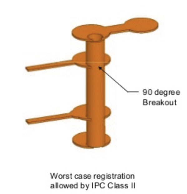
Figure 2. Breakout is expected in Class II PCB layouts. (Source: Viasystems)
Monte Carlo simulations: Gaming the system. We could come up with random numbers that permit natural variation of the location of the relevant ground planes and their adjacent layer traces. A worst-case scenario on one layer meets a worst-case scenario on the next layer very rarely in the real world, but it happens.
By worst case, I mean as far out of specification a layer can be while still meeting the misregistration requirements set forth in the design. If we could have tooling holes with plus/minus zero on both size and positional tolerance, this stuff would be easy, and our monitor would depict the actual nature of the boards. Of course, even non-plated holes have their tolerances. For this reason, I like to have a little more of a buffer around the via on the trace layers. Where possible, using a via-to-line spacing rule that is a little more than the via-to-shape rule will keep the trace from ending up over a void when accounting for misregistration. You can use the same value for both, route everything and never see a design rule violation.

Figure 3. Start with three queens and see how many times you can fill the dance card by playing the same hand 100 times. Modern video poker allows such scenarios. We set up the parameters and get the results in production. Good luck.
In our imperfect world, that is a recipe for routing over those voids by just a little. When you look at simulations of a high-speed line running next to a void, the EMI fields will be more prominent near the broken plane. Tiny discontinuities add up, especially with analog designs. Higher bit rates start to look like RF traces too, so no one is safe from natural variation.
Parallelism and crosstalk. Running traces in parallel causes crosstalk. Using the minimum manufacturable spacing is fine over the short haul. Even a little bit more space means a lot. I just finished a board where I used 5-mil traces for the default non-impedance-controlled line width, then changed all of them to 4 mils once everything was routed. Four mils is enough width for innerlayers, while reducing the metal, and thus the amount of overall radiation of the system. Going from 5 to 6 mils on the air gap reduces crosstalk considerably, since crosstalk is a squaring function rather than a linear one. A little space goes a long way.
Emissions and susceptibility, the two tenets of de-sense, are both favorably impacted by this approach. Down the road, that cumulative space will not be wasted. Going that extra mile also preserved a tiny bit of open space that could be taken on Rev 2, where it seems inevitable we will add a signal somewhere among those traces where there is just enough extra air gap – and then some.
John Burkhert Jr. is a career PCB designer experienced in military, telecom, consumer hardware and, lately, the automotive industry. Originally, he was an RF specialist but is compelled to flip the bit now and then to fill the need for high-speed digital design. He enjoys playing bass and racing bikes when he's not writing about or performing PCB layout. His column is produced by Cadence Design Systems and runs monthly.


