An analog world is where we live. A digital world drives our data.
On the heels of the power distribution network is any analog blocks. If you don’t use minimum component spacing for the entire RF chain, expect blowback from the engineers. I do that placement on a one-mil grid or even less because I expect a lot of scrutiny on analog placement. Why? Simply put, because it’s not digital.
Digital circuitry translates to yes and no (it works well enough or it doesn’t), while analog is a grayscale from zero to infinity, where we’re always chasing a fraction of dB of isolation or some other metric on a sliding scale. It’s a different mindset and analog circuits should be prioritized as much as possible.
Figure 1 shows an op amp in an 8-pin DIP package. It would have a feedback resistor as close as possible to two of the pins and a bypass capacitor between VCC and GND. Two leads are on the input side with polarity and one output pin. Any of those I/O pins could be enhanced with an RC filter or something similar.
Figure 1.A mic, a speaker, a few terminals and an op amp with its constituent passive components; this is a core analog circuit. Aside from audio electronics, these types of amplifiers are common in current sense applications used on eval boards. (Source: University of Bath)
Every part would be on the topside and have leads going through the board. That’s what analog meant when I got into this game. What once fit in a suitcase now tags along in a back pocket and operates completely wireless. The shrinkage of our electronic devices is astonishing.
Figure 2.Half my PCB curriculum was spent on analog design. That’s good because more than half of my career was also spent on these things.
While antenna theory is still in effect, the means of transmitting signals has gone parallel for broadband network access. Analog signals are typically digitized then chopped up and sent over multiple frequencies to be assembled back into media on the user end. Multiple input and multiple output (MIMO) radio sets are a common way of increasing bandwidth.
Shielding is inevitable when condensing lots of applications in a enclosed space. A large sector of the consumer goods industry involves multifunctional IoT devices, where low power consumption is closely tied to some form of wireless communication. While I may not be battery operated, my life seems so. Among my phone, laptop, camera and car, which has better GPS?
Figure 3.Here, we are checking for relative propagation delay and differential pair integrity while setting aside any warnings regarding net schedule, impedance, layer sets, unrouted nets and minimum delay. (In this ECAD view, we’re dealing only with electrical constraints.)
As the timeline progresses, the resonant frequencies of a few GHz made room for 60GHz “WiGig” for close range applications. The 5GHz radios are equivalent to ethernet speed while 60GHz bands are taking market share from the HDMI camp. It may be wise to implement these radios as modules that sit on their own substrate and use the tiniest of components that would drive cost if implemented on a larger board.
So-called front-end modules are an industry of their own. The complex matching networks for the MIMO radio schemes are packaged as a unit. They cater to any number of commonly used receive and transmit chains.
There’s an industry surrounding the notion of a Front-End Module (FEM) where the typical matching networks for a MIMO radio are all on a single, rectangular board mounted to a through-hole or surface-mount motherboard. This would streamline production by consolidating these component-intensive circuits on a manageable component footprint. The board would not necessarily benefit from exotic material and the miniaturization that goes with RF circuit boards.
Let’s double up on the data rates. I would rank memory as a strong second place in the hierarchy of placement and routing. The most sensitive layout memory is the type that is using both the up and down swing of the clock to regulate the data rate.
Known as double data rate (DDR) dynamic random access memory (DRAM), it has more going on than other types of memory, be that serial peripheral interface (SPI), embedded multi-media card (eMMC) and so on, as those types are for storage rather than computing. The complexity of DDR manifests in numerous lanes of data and address buses along with a reference voltage supply and other esoteric nets.
DDR memory is segmented into several bytes, typically eight bits (nets), each with its own timing requirement within the byte lane and in relation to other byte lanes, though to a lesser extent. Two bytes form a so-called “word” for a total of 16 bits.
Four bytes equals two words, or a “double word,” equivalent to 32 bits. A “quad word” is good for 64 bits. This structure permits parallel processing, enhancing system performance. As a result, significant time is spent generating match groups with potentially overlapping constraints. You’re tuning lane to lane as well as within each lane.
Figure 4.The yellow segments indicate we have exceeded the maximum uncoupled length with all the phase matching bumps for the clock pair. My first move would be to use arcs instead of diagonal bumps. We could also pull the jogs closer together for better coupling. If all that fails, see if the spec can be waived to allow what is on the board to stand.
Note that when dealing with length matching of the clock, it can give DRC errors indicating it is both too long and too short. That means that the problem may not be with the clock, but with other members of the bus, with some too long and some too short.
Always phase-match clock pairs using your best effort to center-cut the meter. This provides the greatest amount of leeway for the other traces in the bus to meet the target length (Figure 5). The individual traces must match both legs of the clock diff-pair to within spec. There’s more latitude when the positive and negative traces are the same length.
Figure 5.The phase tuning bumps were removed which cleared up the uncoupled length error. The result is that the negative side of the Clock diff-pair has to be lengthened by ~28 mils to recover the phase matching to within 5 mils.
The number of nets in a DDR memory bus is substantial, especially compared to the other types. A rule of thumb for setting up constraints is that a chip with fewer data lines typically requires a tightly controlled timing budget.
Meanwhile, DDR generally has timing flexibility, especially between byte lanes, with most of the effort going into length matching within individual lanes. As I pointed out, bytes can be combined into words, where the number of members in each group doubles and doubles again until the requirements are met for high bandwidth memory. So far, we have looked at components whose placement is determined by the mechanical considerations followed by decoupling capacitors, crystals, RF chains and memory. The fourth pillar of important placement concerns items that are especially sensitive to outside interference.
While WiFi, Bluetooth, GPS, NFC and others fall under the RF domain, other types of sensors require more board space than their size would suggest. Microphones, pressure gauges, Lidar sensors, compasses and other sundry items require a wide berth that could very well extend through the entire board as well as outward on the surface.
Figure 6.Now the clock net is fully compliant within the pair and with all the single ended memory lines that use the clock in question. The uncoupled length was washed out with the rounded “speed bumps.” While I’m straying from the theme of placement here, be aware of critical nets as you do placement.
The device may benefit from being placed in a quiet corner of the board. It may require its own power supply which should be in the vicinity but out of the line of fire. Special treatment may include provisions for pulling heat away from the device. Power may come in on more than one layer so that the shapes occupy a narrow corridor that doesn’t get corrupted by outside interference. Placement time is also fanout and route planning time.
The engineers on the project may not have the resources or time to analyze a placement without understanding the whole context. If you’re doing the placement of the critical analog parts properly, then the routing should be straightforward.
I would normally make those connections and even pour copper around them before sharing with the team. At least, they can see what you have only visualized. I’d go so far as to populate ground vias along the path so the space is claimed and the EEs can see you want what they want even before they have a chance to say so.
Figure 7.When the official plan is to route the DDR on an outer layer, space must be set aside for that purpose, as it expands from the number of traces and required spacing. This along with any analog connections is high priority as routing ultimately drives placement in these cases.
One of the best things I ever heard from the EE was that he would make a list of things he wanted from the previous submission only to find that those things were addressed with another iteration before he could compile the requests and send them to me. Push out your work early and often so that you don’t get ahead of yourself. Try to think ahead of where they would go with that version and take initiative. You will earn their respect by being proactive. At some point, I would even tape the board out so I can clear up any roadblocks that may be lurking in the design.
John Burkhert, Jr. is a principle PCB designer in retirement. For the past several years, he has been sharing what he has learned for the sake of helping fresh and ambitious PCB designers. The knowledge is passed along through stories and lessons learned from three decades of design, including the most basic one-layer board up to the high-reliability rigid-flex HDI designs for aerospace and military applications. His well-earned free time is spent on a bike, or with a mic doing a karaoke jam.
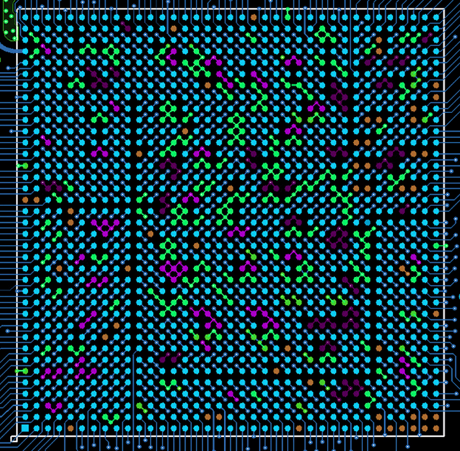
As the devices shrink in pitch and increase in pin count, current density becomes a concern. The outer rows of devices typically have lots of signal pins, while center pins focus on power and ground. This situation means that designers must reserve the first few layers of the board specifically for fan-out (Figure 1).
Figure 1.Just your average 1,369 pin FPGA using a 1.27mm (0.05”) pitch. In terms of colors, green indicates the primary ground domain. Deep purple represents where heavy metal is desired for high current. The lighter magenta is a lower wattage, more spacey kind of metal (like Pink Floyd). Orange marks the no-connect pins.
One of the worst mistakes when dealing with a BGA of 1,000 pins is to drop a via deep into the board for pins on the device’s edge. Be ready to use every lane of the first three layers, and route layer 2 through the air gaps between the other two.
The point is to get away from the device until the trace gets a chance to join the normal flow of the routing channels. You have two distinct areas: the fan-out zone and everything else, where routing up, down, left and right makes sense (Figure 2).
Figure 2.The first thing is to address the outer ring(s) where the top layer is used to escape to a via for the internal routing layer or to a nearby component that is placed there for that reason. The arrows indicate the fan-out flow, always away from the core. For the sake of rework (and room for the fan-out), a component-free area around the device will make it easier to desolder if it needs to be replaced. Otherwise, the tech has to remove the nearby components first.
Find your beach and drop a via that takes you to a level where the current is going your way. Until the vast majority of connections are handled that way, routing between component clusters makes no sense. Fan-out is early in the timeline and updates to the schematic are probably on the table. It’s much easier to move or edit a group while isolated from the rest of the board.
Route the outer ring of pins to “anywhere but here” using the outer layer of the board. If space permits routing between the pins, then the second ring of pins should also escape on the outer layer. If there is no room for that, like with a 0.4mm pitch, then the next layer down is the best option, even if it’s the traditional ground layer.
Conventional wisdom suggest routing orthogonal to traces on the adjacent layers. In reality, that’s a nonstarter on the edges of a pin field. The right routing direction radiates far enough away from the center of the device to connect to components placed around it or to a via where we can start adhering to regular routing according to each layer’s purposes.
Figure 3.This trace in red is eating too many vertical routing channels. One option is to drop a via in the upper left corner and wrap around the differential pairs on the horizontal routing layer. The other option is to use the same brown layer all the way and follow the arrows on the right, routing under the FPGA to the point where only two traces pass through the fan-out vias. From there, routing goes all the way around the high-speed lanes. The first option seems like less work.
Figure 4.The strategy around horizontal and vertical routing layers is knowing when to break away from the trend. The little box full of dangling lines has enough lanes to proceed with a minor revision to the trace. Obstacles such as shields, slots and board edges can be a place to route counter to the prevailing directions as a matter of necessity.
If a PMIC device has external oscillator pins, they are likely buried deep inside the BGA pin field rather than on the perimeter where we like them. Are you going to have headroom for a crystal on the far side of the board? Some internal routing might be involved in getting to the crystal.
In that case, I recommend using a guard band around those traces. Like almost every other component, placing the PMIC near the SoC makes sense. This practice minimizes signal degradation, similar to how engineers position a single regulator near the pins that use the power supplied to any chip. In the case of a PMIC, such concerns are numerous.
With the power domains and essential routing behind us, we can finally close the schematic and play connect the dots using the two innerlayers for vertical and horizontal routing lanes. The unrouted segments have no remaining length or width requirements. My guess is the average person would think this is the nature of most, if not all, routing solutions. This belief has become less common as the percentage of constrained nets has grown over time.
Figure 5.Both power domains can be connected without overlap. If it weren’t obvious before, it’s now clear we can supply the two main power domains with shapes on this layer based on the routing study. The shapes will fill in to distribute the voltages with minimal neck-down. (As we would most likely be using dynamic copper for the power planes, the traces would remain as a backbone. Although they are not close to sufficient in terms of width, they will prevent a future trace from splitting the plane entirely, in case additional routing ends up on this layer.)
Closing those last traces can be a chore as all the good routing channels seem taken. Sometimes, the routing goal becomes “anywhere but here.” You might start at both ends and route a meander as far as it goes in any direction. Along the way, you might have to be “impolite” with the existing work. If the two ends can cross each other at some point, then the routing solution is only a via away. On a 95%-routed board, that still may be a problem. I remember spending 20 minutes clearing out space to add one ground via. Such is life under an NFC chip of a phone.
The fan-out is a chance to make minor adjustments to the placement. This effort continues throughout the fan-out and routing steps. There’s always some guesswork as we go about making design decisions. We’re not always right, but we’re always ready to make it right when new information comes to light.
Figure 6.Re-examining this unused MIPI corner getting two more vias out of the grid. If only one trace may be routed between pins/vias, ensure you do just that. Get a trace through every gap. We can depressurize inner layers in the same way. This applies to pin grid connectors as well as BGA devices. Maximizing each layer’s number of connections is how layer count is reduced to something more feasible.
Preliminary routing. Cross-probing and selectively displaying or colorizing nets provide insight into what’s to come. Although we’ve checked off on the placement gate, it’s a good idea to maintain elasticity for as long as possible. Modularity proves useful when the inevitable update makes it necessary to relocate or rotate a device and its constituent parts.
That said, we must begin connecting the various devices at some point. The heaviest hitting device on the board is a good place to start. It could be key because it uses the most power or has the most interconnects. It may also be the main amplifier or whatever motivates the product. Every board has a device at its heart, so that’s where risk management begins. We must start somewhere.
Step one is the highest priority net on the highest priority chip. It will all be downhill from there; working toward the least significant connections. Operationally, I might not even place pull-up resistors until I complete the pin-escape from the device. Once the trace is fanned out and routed to a clear spot for the via, land the low priority part can land. The same can be said for test points. Get away from the dense area and find a home for the test point.
Figure 7.At times, everything else must step aside and clear all layers for a printed antenna. I use a net short property to tie the antenna shape and the ground via so that the two can coexist at DC and the antenna’s frequency. Like most of these slides, this is made entirely from scratch. The takeaway: Ground vias are always in demand around features like this one.
Like going back to the good old days, we’re using the organic, free-range kind of intelligence that comes straight from our brains. Sometimes it helps to flip the bit. Mirror the board’s image. Soften the color palette. Make it easy on yourself. I hope many of you remain blessed with the option to work from home.
Either way, consider via stubs when doing the fan-out. If the chip is on layer one, then you should use the higher layer numbers for diff-pairs and similar routing. If the route is on layer 3, a stub will run from 3 to the bottom. Avoid back-drilling whenever possible, as it can become a signal integrity thing as layer count increases.
John Burkhert, Jr. is a principle PCB designer in retirement. For the past several years, he has been sharing what he has learned for the sake of helping fresh and ambitious PCB designers. The knowledge is passed along through stories and lessons learned from three decades of design, including the most basic one-layer board up to the high-reliability rigid-flex HDI designs for aerospace and military applications. His well-earned free time is spent on a bike, or with a mic doing a karaoke jam.
Being a manager isn’t for everyone. In addition to technical skills, a manager is responsible for resource allocation and risk management. In the field of electronic design, a manager must balance being a technical person and a people-person. Beyond that, a manager overseeing employees involved in creative endeavors must comprehend the uncertainties and challenges that arise with an electronics design project. Of course, the electrical engineer will normally say the schematic is complete on the day it is supposed to be. Same goes for the mechanical engineer. Ever the optimists, they believe everything is going according to plan – until the day it isn’t. Surprise! (Though, honestly, it’s not really surprising.)
Memory comes in different types, and one key distinction is whether the memory remembers anything once the system is shut down. Nonvolatile memory stays around for the next session, while volatile memory lives up to its name and melts away between uses.
Read more: Implementing Flash Memory in PCB Design


 An analog world is where we live. A digital world drives our data.