 How to calculate trace length from time delay value for high-speed signals.
To keep a good high-speed signal quality from driver to receiver on a PCB is not an easy task for designers. One of the most challenging issues is managing the propagation delay and relative time delay mismatches. To manage the time delays, we need to know how to calculate trace length from time delay value in order to implement the PCB trace routing accordingly. Let me take you through the process.
Calculating signal speed. According to physics, electromagnetic signals travel in a vacuum or through the air at the same speed as light, which is:
Vc = 3 x 10⁸M/sec = 186,000 miles/sec = 11.8 in/ns
A signal travels on a PCB transmission line at a slower speed, affected by the dielectric constant (Er) of the PCB material. The transmission line structure also affects the signal speed.
There are two general PCB trace structures*: stripline and microstrip (FIGURE 1).
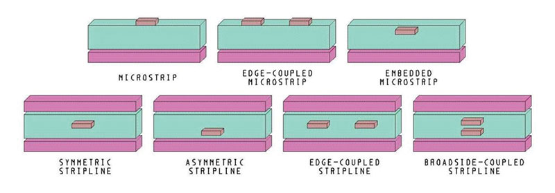
Figure 1. Sample striplines and microstrips.
The formulas for calculating the signal speed on a PCB are given below:
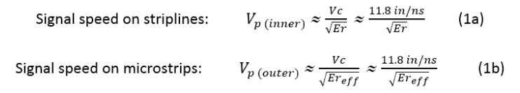
where
- Vc is the velocity of light in a vacuum or through the air
- Er is the dielectric constant of the PCB material
- Ereff is the effective dielectric constant for microstrips; its value lies between 1 and Er and is approximately given by:
Ereff≈(0.64 Er+ 0.36) (1c)
With those formulas, we know the speed of signals on a PCB is less than the signal speed through the air. If Er≈4 (as with FR-4 material types), then the speed of signals on a stripline is half that of the speed through the air; i.e., it is about 6 in/ns.
Calculating propagation delay (tpd). The propagation delay is the time a signal takes to propagate over a unit length of the transmission line. Here is how we can calculate the propagation delay from the trace length and vice versa:
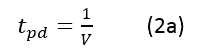
where
- V is the signal speed in the transmission line.
In a vacuum or through the air, it equals 85 picoseconds/inch (ps/in).
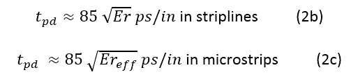
On PCB transmission lines, the propagation delay is given by:
Case Study
To comply with JEDEC specifications, the maximum skew among all signals shall be less than +/-2.5% of the clock period driven by the memory controller. All the signals of SDRAM are directly or indirectly referenced to the clock.
In the example below, the normal FR-4 material with Dk of 4 is used on the PCB with a differential clock rate of 1.2GHz (i.e., 833ps clock period).
Question: What is the maximum skew of the trace length for all the signals?
Answer: Max skew in time delay = +/-2.5% of the 833ps clock period = 20.825ps FR-4 Er≈4, Ereff≈2.92.
So, for striplines, the maximum skew should be less than +/-(20.825/(85*SQT(4)) = +/-0.1225 in = +/-122.5 mil.
For microstrips, the maximum skew should be less than +/-(20.825/(85*SQT(2.92)) = +/-0.1433 in = +/-143.3 mil.
*Note: Different microstrip and stripline structures will affect the signal speed, but only slightly.
Keep this in mind the next time you calculate trace lengths. It should make the job a little easier.
Bibliography
1. Atar Mittal, Signal Speed and Propagation Delay in a PCB Transmission Line, protoexpress.com/blog/signal-speed-propagation-delay-pcb-transmission-line/.
2. JEDEC, jedec.org.
Lance Wang is a solutions architect at Zuken (zuken.com) This email address is being protected from spambots. You need JavaScript enabled to view it..


