Knowing the right geometries is a crucial start.
Simulations are designed to mimic reality and allow exploration of possibilities without building prototypes. This is particularly useful in electronics design, where building a prototype is a highly complicated and expensive task. In order to provide that value the simulation must be accurate, and for signal integrity analysis that means generating accurate models of boards and chips. If everything is done well, a simulation can provide an extremely accurate prediction of what will be measured once the board is built.
The first step to an accurate simulation is a correct board stackup, which is actually an area of continued research and refinement. At the most basic level, the simulation tool needs to be fed the correct trace and dielectric geometries, as well as the dielectric characteristics, namely the dielectric constant (εr or Dk) and loss tangent. This requires a good relationship with material vendors and board houses so the materials used in the board design, and their true characteristics, are understood. The effect of the manufacturing process, including etching and laminating multiple dielectrics together, must be included as well.
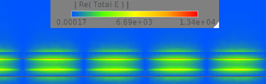
Once this information is fed to the simulation tool, a set of electromagnetic solvers is used to generate the electrical characteristics of the board structures – like traces, planes and vias – from their geometries and material properties. Different types of EM solvers are optimized for solving different kinds of structures. A two-dimensional solver can be used with a very fine mesh to generate accurate models of a trace cross-section very quickly. Planar or 2.5D solvers can solve for power distribution network (PDN) characteristics, as well as generate accurate single-ended via models, which are highly dependent on the PDN as their return path. 3D solvers are best used for irregular structures such as differential vias that are smaller in size. Since the 3D solver is solving for fields in all three dimensions, it is substantially more computationally intensive, so it becomes impractical for larger structures or anything system-level. For optimum accuracy, a “decompositional” approach should be used, which involves using a mixture of solvers for the different board structures. An example of a decompositionally extracted interconnect is shown in FIGURE 1 and compared to measured results. Vias and connectors were solved using a 3D solver and connected to trace models solved with a 2D solver. There is very good correlation up to around 35GHz, which is sufficient accuracy to simulate 25Gb/s signals accurately.
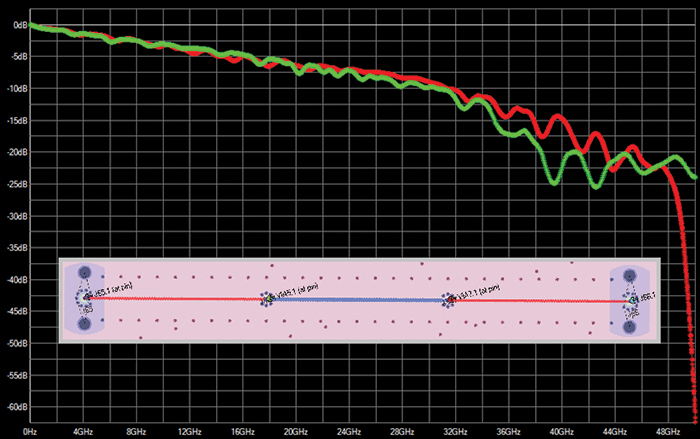
Figure 1. Insertion loss plot generated from simulation in HyperLynx (green) and VNA measurements (red).
Properly characterizing the interconnect becomes very important and more challenging at higher frequencies, where margins are smaller and accuracy crucial to understanding system performance. Another unique challenge brought about by higher frequency busses is the inability to measure them. Because signal wavelengths are so much smaller than the board geometries, connecting a probe to the bus endpoint is now impossible. To permit some measurement, test boards are used for high-speed serial busses like PCI Express. These test boards plug into a standard interface connector and replace the receiver IC with some coaxial SMA connectors, which permit a high-bandwidth connection to an oscilloscope for measuring the system. Because the actual receiver is not used here, the oscilloscope must also mimic the receiver equalization to show the equalized waveform and give a useful indication of pass/fail and system margins.
This is actually one area where simulation presents an advantage; it allows you to look anywhere in the circuit. You can see inside of ICs, past the equalization, and see what the signal would look like at the receiver for the actual system being simulated. Another advantage of simulation is that it zeroes in on a worst-case condition.
Due to challenges measuring multi-GHz waveforms on an oscilloscope, some standards rely increasingly on measurements of the passive interconnect, which can be done with a TDR or VNA. These measurements are typically S-parameter data (FIGURE 2), which can be analyzed in their native form, converted to different
metrics, or applied to certain algorithms to predict system performance. One such example is Channel Operating Margin or COM, which is used by a number of Ethernet standards to predict performance. COM makes some assumptions about the driver and receiver, since they are constrained by the spec, and performs an analysis on the interconnect S-parameter to generate pass/fail criteria. This same analysis can be performed with a measured or simulated S-parameter.
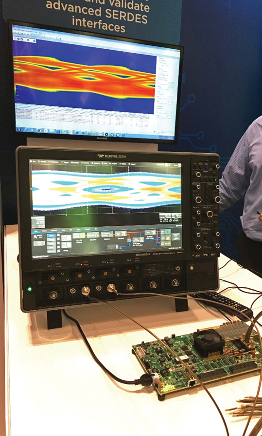
Figure 2. Test board running data patterns measured on an oscilloscope and compared to simulated results from HyperLynx.
Whether measurements are taken on the passive interconnect or on a powered system running data traffic, a simulation can be performed to match the results. Achieving high degrees of correlation requires proper understanding of the stackup and materials, the right solvers, and a simulation tool that brings it all together. The reward for such attention to detail is being able to predict the performance of an electronic system, make design tradeoffs, and fix problems in a fraction of the time and cost it would take to build and test a single prototype.
Patrick Carrier is product manager for high-speed PCB analysis tools at Mentor Graphics (mentor.com); This email address is being protected from spambots. You need JavaScript enabled to view it..