Don’t panic. Several options exist for suppressing or containing unwanted emissions.
Your product has failed electromagnetic compatibility testing. Now what do you do? Several options usually fall into the category of either containment or suppression. Elimination is probably the best option, but it can often be difficult to track down the problem to eliminate it. At the very least, you should be questioning how you got to this point and what can be done on the next design to prevent it.
Containment. Containment is probably the most “brute force” method of solving emissions problems. If the design is radiating up to a certain frequency, it can be kept in a metal box. Ideally, the metal box would be sealed on all sides, but unfortunately there also needs to be some airflow. So, the holes for airflow need to be smaller than the wavelength of the highest frequency to be contained. This creates what is called a “Faraday cage” around the board to prevent unwanted emissions from escaping. This means any doors or other box openings must have metal gaskets to maintain electrical connectivity around the entire box when closed. A great example of this is a microwave oven, which has a perforated screen on the front for viewing food as it cooks, with holes small enough to prevent the microwave radiation from escaping.
Unfortunately, it is often difficult to put a design in a completely enclosed metal box. Another option is to implement a Faraday cage at the board level. This is usually done by routing wide traces (usually ground) around the perimeter of the board on the front and back sides and stitching them together with vias. An example is shown in Figure 1. This creates apertures consisting of the vias and the top and bottom shield traces, which can be made small enough to keep high frequencies from radiating out of the board in the x and y directions. This would include all “inner-layer” radiation, including radiation from signal vias without sufficient stitching and signals crossing gaps in planes (two practices that should actually be avoided – more on that later). It is generally assumed any radiation in the Z direction will be shielded by the solid planes, usually on the second layers in. This leaves only the radiation of the outer-layer traces, which should be minimal if those second-layer planes are kept solid and continuous. Verification that the perimeter traces do in fact completely encircle the board and that stitching vias are appropriately spaced can take a great deal of time, especially if checked manually. By using an automated check, verification of these structures can be completed in a matter of seconds (Figure 1).
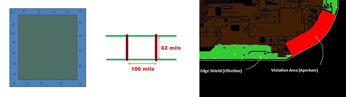
Figure 1. Depiction of Faraday cage on a board; side view of resulting apertures; results from running Edge Shield DRC shown in Mentor Graphics’ HyperLynx DRC.
Suppression. Trying to contain EMI usually requires substantial effort, effort that might better be spent trying to suppress the problem. The other issue with “containing” radiated emissions is that they are still affecting other parts of the design, not to mention that if energy is radiating, it is being lost from the transmitted signal, which will manifest as signal degradation. Using techniques such as spread-spectrum clocking (SSC) to spread the frequency content of the signals such that their radiation levels are reduced is a common suppression practice. The most effective method, however, is to eliminate the board structures causing the radiation. Since the offending signals obviously need to be identified before employing something like SSC, those signals can be examined to determine the cause of the radiation.
Quite often, radiation is caused by broken return paths for signals. Current wants to travel in a closed loop, and if that loop is broken, an antenna is created. Two of the most common examples on board designs are signal vias without stitching and traces crossing reference plane splits.
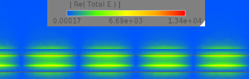
Any time a signal transitions layers, its return current must also transition layers. This is essential to maintaining a tight current loop for the signal, to keep energy from radiating. The further the transition via, the higher the impedance (inductance) added to the return path (FIGURE 2). The higher the inductance added to the return path, the more high-frequency energy gets radiated.
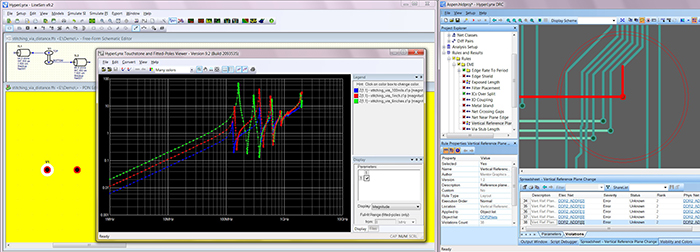
Figure 2. Increasing bypass impedance from larger stitching via spacings shown in HyperLynx PI; results of Vertical Reference Plane Change DRC from HyperLynx DRC.
Another way to look at it is that the higher the signal frequency, the closer the stitching via needs to be. Adding more stitching vias reduces the bypass impedance even further. Ideally, every signal via would be surrounded by a ring of stitching vias, but that is often not practical. If a signal is transitioning from referencing a ground layer to referencing a power layer, a stitching capacitor must be used instead of a via, which will end up adding much more inductance to the return path, but is certainly much better than no stitching at all.
Obviously, layer transition vias cannot be eliminated from designs, but they can be made to radiate much less by the addition of stitching vias (or caps). Even better is to run signals completely on one layer, which puts the “layer transition” right at the ICs. These are good places for layer transitions, as they typically contain large numbers of ground and power vias, which act as stitching. The ICs also tend to be surrounded by decoupling capacitors, which also act as stitching capacitors.
Another common example of broken return paths is traces crossing plane splits. This is similar to changing reference planes through a via, except the reference is changing from one plane to another on the same layer. Since the planes are at different potentials, this means capacitors must be used as stitching components.
Since a mounted capacitor is a narrowband structure, a number of capacitors would ideally need to be used to “correct” this problem. A much better solution is to move the signals or the splits to avoid this kind of situation. This is often very difficult to do in later design stages, so careful plane planning during the early stages of layout is the best time to address this.
Capacitors are also vital to minimizing other less obvious breaks in return paths. As I/O buffers transition from 0 to 1 and 1 to 0, current must make its way between power and ground. The capacitors at the IC complete this path. These capacitors actually serve dual roles as both decoupling capacitors, providing local high-frequency current to the ICs, and bypass capacitors, providing continuous AC current paths. An AC analysis (a.k.a decoupling analysis) of the board power distribution network (PDN) can reveal any high-impedance resonant points in the board PDN (FIGURE 3).
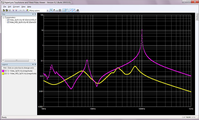
Figure 3. Results of an AC (decoupling) analysis of a board PDN, shown in HyperLynx PI.
If a board PDN has any very high-impedance resonant points, that can indicate a possible radiation risk at those same frequencies. The lack of a low-impedance return path for signals at the ICs means energy will be radiated as EMI. The PDN should be modified to suppress the resonant points, which usually means the addition of a number of capacitors. However, improvements to the way the capacitors are mounted or changes to the board stackup can also yield favorable changes to PDN performance.
Patrick Carrier is product manager for high-speed PCB analysis tools at Mentor Graphics (mentor.com); This email address is being protected from spambots. You need JavaScript enabled to view it..