Backdrilling is a cost effective strategy to reduce detrimental signal distortions cased by PTH via stub structures.
Plated through-hole (PTH) via structures in high layer count printed circuit boards and thick backplanes/midplanes can significantly distort high-speed digital signals that pass through them. Often the distortion is severe enough that digital receivers can no longer ascertain whether a logical one or a logical zero was originally transmitted. As data rates increase, the amount of distortion introduced by the PTH via structure also increases, usually at an exponential rate considerably higher than the associated increase in data rate. For example, the distortion producing effects of a PTH via at a 6.25 Gb/s data rate is often more than double that at 3.125 Gb/s.
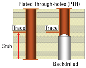
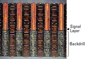
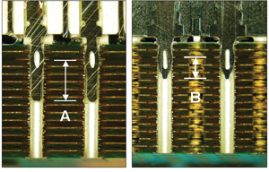
A dominant structure within a PTH via that introduces this undesired distortion is the via stub. The via stub is the conductive portion of a PTH via not connected in series with the circuit (Figure 1). Since a via stub serves no useful function in the circuit, it can be removed using a technique known as backdrilling. Backdrilling uses controlled depth drilling techniques that are compatible with conventional NC drill equipment. Essentially, a drill bit slightly larger in diameter than the one used to create the original via hole is used to remove the undesired conductive plating in the via stub region. Figure 2 shows a cross-section of PTH vias that were backdrilled.
|

FIGURE 1. Backdrilling to remove a via stub.
|
|

FIGURE 2. Cross-section of backdrilled PTH vias.
|
Decreasing via stub length by backdrilling significantly reduces a particularly problematic form of signal distortion called deterministic jitter. Because bit error rate (BER) is strongly dependent on deterministic jitter, any reduction in deterministic jitter by backdrilling will significantly reduce the overall BER of the interconnect – often by many orders of magnitude. Other key advantages to backdrilling PTH vias include: less signal attenuation due to improved impedance matching, increased channel bandwidth, reduced EMI/EMC radiation from the stub end, reduced excitation of resonance modes, and reduced via-to-via crosstalk.
How Via Stubs Distort High-Speed Signals
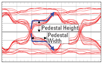
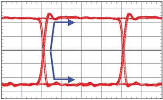
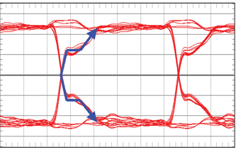
Figure 3 and Figure 4 show representative eye-diagrams of two via structures, one with an intact stub and one without a stub. Comparing the two figures, one can see that via stubs introduce horizontal pedestals in the logic 0 to 1 and logic 1 to 0 transitions. These pedestals close the eye, making it more difficult for the digital receiver to ascertain whether the received signal is truly a logical one or a logical zero.
|

FIGURE 3. Via stubs introduce horizontal pedestals into the logic transitions resulting in eye closure.
|
|

FIGURE 4. “Stubless†vias have clean logic transitions and correspondingly larger open eyes.
|
The “height†of the pedestal is proportional to the equivalent impedance of the stub. A higher via stub impedance results in a higher, more desirable, logic 0 to 1 pedestal level (and a corresponding lower logic 1 to 0 pedestal level). An effective way to increase stub impedance is to decrease shunt capacitance by removing non-functional pads and increasing anti-pad diameters. While these techniques help, they are often not enough to reduce distortions to acceptable levels.
The width of the pedestal is proportional to the length of the stub. A short stub produces a narrower pedestal width and a correspondingly wider, more useable eye. An easy way to reduce the width of the pedestal is to decrease the overall length of the via stub by backdrilling. Figure 5 shows an eye-diagram of a properly backdrilled PTH. One can readily see that the residual stub length remaining after the backdrilling operation results in a significantly larger eye opening.
|

FIGURE 5. Backdrilled vias have significantly reduced pedestal widths and significantly larger eye openings.
|
It should be noted that alternate construction techniques such as laser-drilled vias, and alternative stack-up arrangements where traces are moved to layers closer to the end of the via stub, can also be used to reduce stub length. But in many high-density printed circuit boards and backplanes/midplanes, these options are not always viable from both manufacturing and cost standpoints. In this case, the only option is to remove the via stub by backdrilling. Of course, stub removal is not the only signal integrity improvement technique that one can apply to the via. Optimization of the remaining portion of the via that is not backdrilled – using for example, the Sanmina-SCI patent pending Opti-Via “via-tuning†algorithm – can further reduce via-induced signal distortions.
How Much Residual Stub Length Can Remain?
Once the decision is made to backdrill, the question of how much residual stub length can remain arises. Does a thick backplane with 17 signal layers require 17 separate backdrill depths? Or are only three backdrill depth levels equally spaced across the stack-up acceptable? The answer depends on several inter-related factors including the desired signal integrity performance and practical (cost-effective) manufacturing considerations and limitations. As a general rule, increasing the number of vias that need to be backdrilled and decreasing the maximum allowable residual stub length will significantly increase the manufacturing costs of the PCB/backplane.
From a signal integrity performance perspective, a 3D full-wave simulation of the backdrilled via structure is often required in order to ascertain the actual impact it has on the desired signal integrity performance. High performance interconnects that operate at either higher data rates and/or lower BER generally require smaller residual stub lengths. For estimation purposes, however, a rough gauge of how much stub can remain can be approximated by modeling the via stub as a lumped element impedance mismatch, and then calculating the percentage signal loss as a result of that impedance mismatch. Table 1 [PDF format] shows the approximate percentage signal loss due to via stub length for a typical 6.25 Gb/s backplane/midplane construction. The eye diagram in Figure 3 was measured on an interconnect having a residual stub length of 15 mils. As a reference point, the signal reflection loss due to a 10% trace impedance mismatch is approximately equivalent to a 20-mil stub length.
It has been our experience that most digital interconnect applications that operate at data and BER less than 10 Gb/s and 10-15, respectively, generally do not need to have their stub lengths reduced to below 10 mils. This is especially true if some form of active or passive transmit-side pre/de-emphasis or receiver-side equalization is incorporated into the overall interconnect design strategy. For example, the Sanmina-SCI full-mesh high perfomance ATCA backplane only has three levels of backdrilling with the largest via stub length being 80 mils long.
Smaller via stubs are always better than larger ones, and so for the sake of expediency, many signal integrity engineers will dispense with the more time-consuming 3D simulations that were supposed to provide the answer to the maximum allowable stub length question and approach the problem from the opposite perspective: Simply require all via stubs be reduced to the smallest length possible. This often leads to an ongoing improvement mentality, where each new PCB/backplane automatically requires a via stub length that is 20% less than the last one that was designed – and a lot of lively happy-hour discussions over whether reducing residual via stubs by an additional 2 to 3 mils actually provides significant improvements in the SI performance of the total interconnect.
The smallest residual stub length one can impose during the manufacturing of a PCB/backplane without accidentally drilling out the pad connected to the desired signal layer is dependent on a number of variables. Unfortunately, not all of these are under the direct control of the PCB/backplane manufacturer. Minimum residual via stub length is dependent on two factors. The first is precisely knowing the Z-axis location of the layers (Z-axis location uncertainty). The more accurately we know the physical location of the signal layer, the closer we can backdrill to that layer. The second is limiting the residual stub length to a value slightly longer than the tolerance associated with the actual drilling operation. Of these two, the latter is generally easier to define and control than the former.
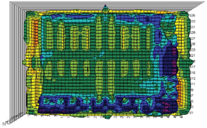
Percent copper coverage has typically shown itself to be one of the largest contributors to Z-axis location uncertainty. Localized regions where a relatively large percentage of the area is uniformly covered with copper requires a smaller resin fill “demand†than regions whose copper features are a relatively small percentage of the area. Areas with small resin fill demands are generally thicker than regions with large resin fill demands. This means the thickness of the PCB/backplane at a particular via location, and consequently the actual Z-axis location of the layers, depends on the percentage copper coverage on the layers above/below the location of the via that needs to be backdrilled. This undesired effect can be minimized through the effective use of thieving, a process that generally requires feedback between the PCB fabrication supplier and OEM prior to manufacturing the PCB/backplane. Adding small pads (typically primary drill diameter – 4 mils) in the via pad stack on layers that will be removed during the backdrilling operation will also help minimize Z-axis variations. Figure 6 graphically shows how localized variations in copper density can impact the overall thickness of a representative backplane.
|

FIGURE 6. Copper fill analysis showing total
copper density across a representative backplane.
|
Another significant factor contributing to Z-axis uncertainty is core and prepreg thickness tolerances. These tolerances add up, resulting in a correspondingly higher level of uncertainty the deeper one drills into the PCB/backplane. This can be especially problematic on PCBs that have a high layer count. Utilization of low resin percent constructions can help reduce incoming material thickness variations.
One way to minimize these Z-axis uncertainties is to drill a series of test holes along the periphery of the panel prior to backdrilling and then do a cross section on the test holes to determine the exact location of the backdrill depth as compared to the exact locations of the PCB/backplane layers. While this technique does not fully compensate for variations in thickness across the panel, it does eliminate a significant portion of the depth uncertainty associated with the backdrilling process.
Most newer drill equipment uses a variety of sensing techniques to ascertain the exact location of the top of the PCB/backplane prior to beginning the drilling operation and, as a result, are capable of meeting a +/-0.001? depth control tolerance relative to the top of the PCB/backplane. As a general rule, Z-axis location uncertainty of a particular layer due to copper coverage and core/prepreg thickness tolerances dominate the amount of residual stub length remaining after the backdrill operation. (At the time of this writing, a high-speed drill bit outfitted with a layer sensor and associated microprocessor based counter adjacent to the crown of the drill bit, capable of counting layers in real-time as the drill penetrates the PCB/backplane, is still a largely unfulfilled dream.)
The bottom line is that current industry-wide practice is to limit residual stub lengths to 10 mils maximum, with stub lengths less than 7 mils incurring an additional manufacturing cost.
Assembly-related considerations can also impact the overall effectiveness of the backdrilling process. For example, press-fit connector tails can act as stubs, negating the improvements afforded by backdrilling out the via stubs. It makes no sense to backdrill a via to remove its stub, and then insert a press-fit connector into the backdrilled via whose tail extends beyond the backdrilled depth (Figure 7a). If this is an issue, then options include replacing the long-tailed connectors with an equivalent connector having much shorter tails, as shown in Figure 7b, replacing the connector with an SMT/BGA equivalent, or moving critical routing layers below the connector tail so the tail becomes part of the non-backdrilled portion of the via.
|

FIGURE 7a) Long press-fit connector pintails can create undesired stubs that backdrilling cannot eliminate and, b) press-fit pins with shorter tails provide improvement.
|
Backdrilling and Routability
The backdrill diameter needs to be slightly larger than the primary drill diameter. The backdrill bit size is usually 8 mils over primary drill size, with 10 mils larger preferred. Trace and plane clearances need to be large enough that the backdrilling process does not accidentally drill through traces and planes located adjacent to the backdrilled hole. Minimum plane and trace clearances (spacings) of 10 mils is preferred.
Practical Guidelines and Suggestions
While some design considerations need to be taken into account, the integration of backdrilling into a PCB or backplane/midplane construction is, to a great extent, an unobtrusive process. One helpful technique that can often aid in more easily identifying which vias are backdrilled to which depths is to identify each unique drill depth through a combination of unique tool numbers in NC files, unique tool symbols on CAD drawings, and specifying slightly different drill diameters for the different drill depths. For example, a backdrill to layer 13 references back drill size 0.01201, a backdrill to layer 15 references back drill size 0.01202, etc.
Backdrilling is a cost effective strategy to significantly reducing detrimental signal distortions caused by PTH via stub structures. Properly executed, backdrilling does not have a significant impact on PCB/backplane reliability or yield. PCD&M
Franz Gisin is director of Backplane Design Technology and Signal Integrity Design in the PCB Operations division of Sanmina-SCI. He can be reached at This email address is being protected from spambots. You need JavaScript enabled to view it.. Alex Stepinski is senior engineering manager at Sanmina-SCI. He can be reached at This email address is being protected from spambots. You need JavaScript enabled to view it..


