Copper-filled microvias, controlled aspect ratios and fabrication-aware design are redefining vias.
If you want a front-row seat to the evolution of PCB technology, look no further than vias. While ultra-fine lines tend to capture the spotlight, real transformation is happening in the via structures that connect those lines from layer to layer.
Vias are no longer simple drill-and-plate features. In ultra HDI, they are engineered elements that require the right geometry, material set and process window to work.
Let’s take a look at what is driving this shift. As BGA pitches slide below 0.5mm and layer counts continue to climb, designers are leaning on microvias that must be smaller, more precise and far more reliable than only a few years ago.
Good interconnects start long before a board hits the shop floor. They begin with a design that accounts for limits, opportunities and the realities of building ultra HDI.
Copper-Filled Microvias
One of the most significant changes shaping UHDI is widespread adoption of copper-filled microvias. In HDI, nonconductive fill was often adequate. As features shrink, electrical and mechanical demands quickly escalate, however. That is where copper fill earns its place.
Copper-filled microvias bring two major benefits:
- They support stacked structures. A solid, planar landing pad provides the next microvia with something stable to sit on.
- They distribute stress more evenly. Copper does not deform as resin does, so the interconnect is better prepared to handle thermal cycling.
From the fabrication side, none of this happens by accident. Producing a reliable copper-filled via requires a well-tuned plating process. Bath chemistry, temperature and agitation patterns all interact to drive a consistent fill. When these are in balance, the via fills cleanly and planarizes smoothly. Copper via-fill isn’t just a material choice. It’s an entire process commitment.
Small Ratio, Big Consequences
Via diameter and depth are often addressed separately, but aspect ratio is the real story. A microvia that’s too deep for its width becomes difficult to plate up evenly and harder to drill cleanly. For ultra HDI, most fabricators prefer aspect ratios of 0.75 to 1:1. Some can push tighter, but only with specifically tailored materials and equipment.
Why does staying within this window matter?
When a via is too deep relative to its diameter, plating uniformity drops sharply and increases the risk of voids and weak spots. Very thin dielectrics also make laser drilling less predictable, complicating depth control and consistency. In addition, debris removal becomes more difficult, permitting residual material to remain in the via where it may introduce long-term reliability risks. Aspect ratio can significantly impact yield. It’s one of those details that feels minor but has a real consequence on the finished board. A little knowledge upfront saves a lot of headaches later.
Stacked Vias
Stacked vias are quickly becoming the norm in UHDI builds, especially when routing channels narrow and there is no room to stagger. Copper fill enables stacking, but it also raises the bar for process control.
Stacked via structures depend on consistent dielectric thickness, so each laser drill can reliably reach its intended depth. They also require precise layer-to-layer registration as spacing shrinks, along with planar, well-filled microvias that remain stable and do not deform during lamination.
When all these elements are aligned, stacked vias deliver impressive density and performance. If a single process step shifts, however, alignment issues or stress concentration become visible.
Stacking is doable and predictable, especially when treated as a precision-engineered structure.
Staggered Vias: The More Forgiving Alternative
While ultra HDI may receive considerable attention for stacked vias, staggered vias are a smart choice in many designs. The structure, offsetting each microvia, permits the dielectric to absorb mechanical strain rather than concentrating it in a single column of copper.
Staggered via structures are especially useful when the dielectric system has higher CTE values or when dielectric thickness varies across the stackup. They are also well-suited for products that experience wide temperature swings and for designs where long-term reliability is more important than maximum routing efficiency. The tradeoff is straightforward: staggering consumes more board real estate. However, for many applications such as wearables, portable electronics or anything facing harsh thermal conditions, the extra robustness is worth the added routing effort.
From a fabrication standpoint, the difference between a via fence and American Standard Circuits’ Via Wall shows up in yield and consistency. A via fence is usually placed for electrical reasons and tolerated as long as it functions. A Via Wall is engineered as part of the build process itself, with tighter spacing and registration intent, giving the fabricator a more stable structure to control movement, drilling accuracy and copper fill behavior as microvia counts climb (Figure 1).
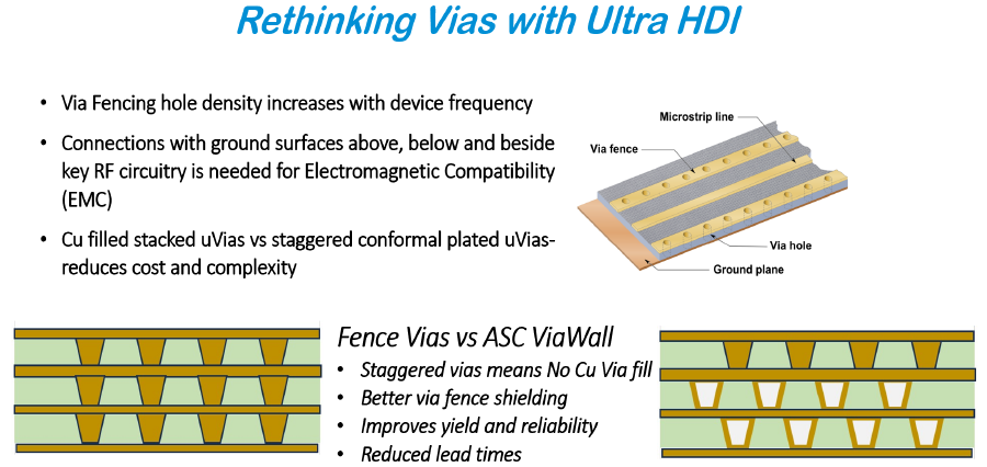
Figure 1. ASC’s novel RF fence via option.
Materials and Via Wall Integrity
Selecting the right materials has always mattered in PCB design, but in UHDI, the margins get tighter. Materials considerations include:
- Dielectric response to laser drilling. With new materials and thin dielectrics, even small variations can begin to affect consistency and depth control.
- Copper adhesion and foil roughness. Very low-profile and ultra-low-profile coppers contribute to signal integrity at high speeds, but do not always give the same kind of mechanical anchoring when compared to rougher foils. That could affect the bonding of microvia walls to the surrounding material.
- Resin recession. During thermal cycling or reflow, resin can pull back from copper. In thin dielectrics, even a few microns of recession can impact via wall support.
It’s not about adding complexity but choosing materials that behave predictably with the processes the fabricator uses.
Designing with Real Process Windows
Innovation is exciting, but implementation takes the prize. The most successful ultra HDI designs grow out of early conversations with fabrication partners. Once their drilling capability is understood, via fill processes, registration tolerances and material preferences, design structures can be designed that build cleanly and yield well.
Practical suggestions:
- Keep aspect ratios conservative, unless the fabricator confirms it can support more aggressive geometries.
- Treat stacked microvias as engineered features rather than just vertical routing lines.
- Material selection aligned with processes for drilling, filling and laminating the board.
- Provide spacing representative of real-world registration tolerances.
When the design intent aligns with the fabrication capability, UHDI becomes predictable rather than challenging. And predictable is what we need when long-term reliability counts.
Takeaways
The via revolution in UHDI is not just about feature-size reduction; it is about a complete ecosystem that permits these small features to perform reliably over time. Copper-filled microvias, precise aspect ratios, well-controlled laser drilling, and thoughtfully chosen materials all work together to deliver designs that hold up under demanding conditions.
Anaya Vardya is chief executive of American Standard Circuits/Sunstone (asc-i.com); This email address is being protected from spambots. You need JavaScript enabled to view it..


