A DfA program that designs and specifies PCBs compatible with lead-free
soldering is often at odds with a cost driven manufacturing metric.
Significant attention and a great deal of effort have been expended
on understanding the reliability of lead-free solder joints. However,
difficulties posed by lead-free soldering as it relates to the
reliability of PCB interconnect structures is perhaps more significant.
Problems with PCB viability after the assembly process comes primarily
from one source – the temperatures required to attach components during
the lead-free assembly soldering process. These reliability issues
required the development of a White Paper1 from which the materials in this article were taken.
With
SnPb soldering, PCB reliability was typically not an issue, but in our
brave new lead-free world, this is no longer the case. PCBs now need to
be designed and specified to be fully compatible with lead-free
soldering. Unless these changes are included in the specification of a
PCB, this will not happen, because PCB fabricators will build based on
lowest possible cost. To carry out the changes needed to assure
lead-free assembly success often comes with an increase in
manufacturing cost.
PCB Base Materials
To
assure the survival of PCBs during the high soldering temperatures and
their subsequent reliability afterward, improvements in PCB resin
properties are necessary. The integrity of the PCB interconnect
structures – plated through-hole copper barrels and barrel/inner-layer
interconnects – requires improved glass transition temperatures (Tg)
and lower coefficients of thermal expansion (CTE). Improvements in Tg
and decomposition temperature (Td) are also necessary for the thermal
stability of the PCB resin.
PCB base and prepreg materials are frequently specified according to industry document IPC-41012.
It should be noted that using IPC-4101 slash sheets for material
choices is not sufficient to specify specific properties. The range of
properties contained in these slash sheets is too broad for this
purpose. It is therefore recommended that specific materials or their
equivalents be specified for critical applications.
The
glass transition temperature should be determined using the
Thermo-Mechanical Analysis (TMA) method, as per IPC-TM-650, 2.4.24C3. This method is preferred over DSC4 and DMA5,
two other methods used to determine the glass transition temperature,
because thermal expansion of the PCB is a critical parameter and is
given by TMA as a function of temperature.
For all but thin PCBs, a minimum decomposition temperature, Td (determined as per IPC-TM-650, 2.4.24.66)
as well as a maximum thermal expansion coefficient in the PCB thickness
direction, CTE(z) (determined as per IPC-TM-650, 2.4.417)
should be specified. CTE(z) values should be given separately for
temperatures below Tg and above Tg, however, thermal expansion (TE in
%) is often given in a range of temperatures from 50 to 260ËšC; good TE
values typically are 3.2% or less. Typically, the decomposition
temperature is given as Td (5%) to a 5% weight loss. A decomposition
temperature of Td (2%) to a 2% weight loss has been found to be a
better indicator, but data based on this parameter is not yet widely
available.
Often, the time to delamination (T-288 or
T-260) is specified, either in addition to Td, or instead of it. The
T-288 delamination time provides a more appropriate level of
performance, given the process temperature required for lead-free
soldering. Delamination time is sometimes combined with the requirement
that the PCB needs to survive the process temperature for 4 to 5
excursions.
Unfortunately, the data sheets from the
various laminate/prepreg suppliers are typically neither consistent not
complete. Moreover, where property measurements were performed by
commercial laboratories (because the values given in the data sheets
did not appear to be credible) the values of the CTE(x) and CTE(y) were
found to be nearly double those given in the data sheets.
When
qualifying laminate materials, during the preliminary search,
elimination and final selection process, the three properties that
critical for the survival of the PCB and the PTH/via interconnect
structure in a lead-free assembly are:
- Glass transition temperature = Tg
- Decomposition temperature = Td, and
- Thermal expansion = TE
These
critical parameters can be combined in a Soldering Temperature Impact
Index, STII, which is defined as STII = Tg/2 + Td/2 – (TE%(50 to 260ËšC)
x 10).
For PCBs with thicknesses of 0.06 inches [1.5
mm] or greater, an STII value of 215 or larger is recommended. The STII
concept is still not widely used, however, many, but by no means all,
base materials offered by suppliers meet and exceed an STII-value of
215.
The reason for the importance of these
properties comes from the thermo-physical loading that the PCB
interconnect structures, such as plated-through holes (PTHs),
plated-through vias (PTVs), buried vias and even micro-vias experience
during the temperature excursions used in the lead-free soldering
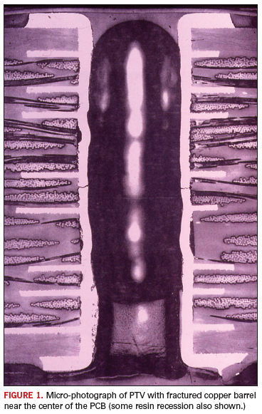
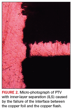
process. Failures such as via barrel cracking (Figure 1) and innerlayer post separation (Figure 2) can be avoided by proper design. The resin recession, shown in Figure 1, does not have any real reliability consequences.


In
order to reduce the z-axis thermal expansion, various fillers are added
to the basic PCB resin systems. In some cases, this reduces the
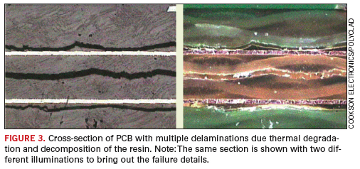
strength of the material and leads to cohesive delamination failures as
seen in Figure 3. Unlike adhesive failures resulting
from a delamination at the copper-to-resin interface, cohesive
delamination is limited to the dielectric material itself.

Desmear
Lead-free
compatible, high-Tg (170-180ËšC) materials often use phenolics as curing
agents. The resistance of these laminate resins to desmear chemistries
is substantially higher than the dicy-cured, high-Tg materials.
Therefore, desmear procedures may require re-evaluation. Any new
laminate material should not be assumed to be a drop-in replacement. If
the desmear cycle has not been optimized, there will be poor hole wall
topography and the potential for residual resin smear and plating
defects.
Design and Specifications
Because
of these issues, new PCB base materials designed for lead-free solder
assembly need not only be properly selected according to their data
sheet information, but also should have coupons tested in the product
configuration to demonstrate their ability to meet quality and
reliability requirements. In fact, some in the industry prefer to
specify the capabilities of the finished product instead of specifying
material properties. The argument advanced is that it is not only the
importance of properties of the raw materials used, but also the impact
of the processing environment that ultimately determines the product’s
success.
Product capability requirements could be
given in terms of the maximum expected temperatures reached during
lead-free soldering processes and total exposure time, for example,
280ËšC for 3 minutes, inclusive of all soldering processes – HASL,
reflow, wave, as well as rework and repair. Alternatively, one could
specify solder floats or dips, for example 288ËšC for 3 to 5 cycles of a
specific time. The coupons would have to withstand these exposures
without delamination, barrel cracking and/or inner-layer separation.
It
has also been suggested that a cyclic “time-to-delamination” protocol
be introduced. So, perhaps in addition to or as a replacement for a
T-260 test, a cT-260 value could be generated by first conditioning the
boards by thermal cycling to 260ËšC or some higher temperature for X
number of cycles, to simulate the assembly process. For example, 6
thermal cycles could be used to simulate 3 reflow and 3 rework cycles.
After the thermal cycles have been completed, the PCB would be
subjected to the standard T-260ËšC testing until delamination occurs. It
has been reported that some “high performance” resin systems degrade
with thermal cycling much more readily than from a single thermal
excursion to 260ËšC or even 288ËšC, and that materials with poor cT-260
results usually do not fail because of delamination, but because of
barrel cracks of the vias.
Non-Functional Lands
A
common assumption has been that the removal of non-functional lands
(NFLs) has no impact on reliability, but this assumption needs to be
rethought in light of the higher lead-free soldering temperatures,
which can reach temperatures of 265 to 280ËšC when soldering with some
lead-free solders.
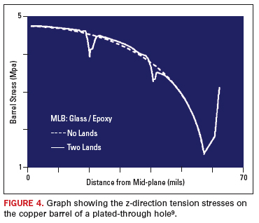
Previously it was shown that there was no significant impact on barrel stresses when NFLs were removed, as can be seen in Figure 4.
However, recent testing has shown the removal of NFL to be nowhere near
as benign for assemblies undergoing the lead-free soldering process as
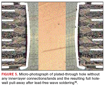
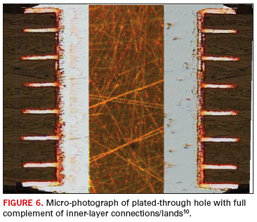
had been tacitly assumed. Figure 5 shows some recent industry experience with PTHs in PCBs that reached the “red flag”-level at an aspect ratio of 4-to-1. In Figure 6,
the same PCB is shown with a full complement of non-functional lands
(NFLs) and it shows no wall separation or resin recession.


Copper Dissolution and Plated Copper Thickness
It
was only recently that the IPC-specification for minimum copper plating
was lowered from 1.0 mils to 0.8 mils [25 to 20 µm]. This was done in
response to the increased costs and time required to plating 1.0 mils
of copper in the center of the hole in high aspect ratio boards. These
cost are associated with the lower plating current densities required
to plate uniform copper into high aspect ratio plated-through vias
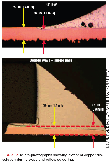
The
higher soldering temperatures, together with the very high tin content
of lead-free solders, leads to a significant increase in the rates at
which copper is dissolved during soldering processes. This can be seen Figure 7.
Reductions in copper thickness by as much as 12 µm [0.5 mils] have been
reported. The minimum copper plating thickness may need to be increased
in light of these finding to perhaps 1.2 mils [30 µm] to allow for the
potential dissolution without a negative affect on PTH reliability.
Increasing the copper barrel plating thickness can improve the survival
and long-term reliability of PCBs that will undergo the higher
soldering temperatures used with lead-free solders, and this increased
thickness will need to be specified by the designer.

Moisture Absorption and Bake-Out
Moisture
absorption can play a significant role in whether a PCB can survive the
high temperatures required for lead-free soldering. Thus, it is
imperative that both test coupons and production PCBs undergo adequate
moisture bake-outs just prior to assembly. These bake-dry or vacuum
bake procedures should be done at temperatures not to exceed 105ËšC for
the number of hours (up to 24) required to sufficiently remove moisture
from the PCBs.
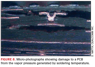
Vapor pressure within the PCBs can
cause both cohesive and adhesive failure modes, depending on where the
weakest bonds are located, whereas thermal decomposition due to
inadequate thermal stability leads predominantly to cohesive failures.
It should be noted that the vapor pressure within a PCB roughly doubles
from 220ËšC to 260ËšC. The consequences of high vapor pressure can be
seen in Figure 8.

Testing
PCB testing using IST (Interconnect Stress Testing) as per IPC–TM-650, 2.6.2611, or HATS (Highly Accelerated Thermal Shock) as per IPC-TM-2.6.7.2B12 assures primarily long-term reliability in terms of operational conditions.


Preconditioning,
such as subjecting a PCB to 5 or 6 cycles of solder reflow or vapor
phase exposure up to the maximum soldering temperature could reveal
possible damage resulting from the high lead-free soldering
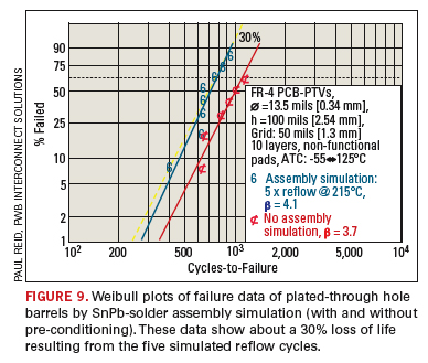
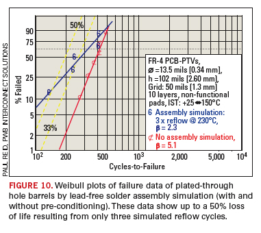
environment. Such preconditioning shows that temperature excursions to
solder reflow temperatures can reduce the PCB long-term reliability by
as much as 50%, as illustrated in Figures 9 and 10.
The difference in the samples in Figures 9 and 10 is the increase in
preconditioning temperature, which is still not at the level expected
for lead-free reflow soldering. PCD&F
REFERENCES
1. Engelmaier, W., “Recommendations for PCB FAB Notes and
Specifications in Printed Circuit Board Drawings for SnPb and Lead-Free
Soldering Assemblies, the Qualification of PCB Shops and Activities to
Assure Continued Quality, v.07,” White Paper/Multi-Client Study,
Engelmaier Associates, L.C., February 2007.
2. IPC-4101 “Laminate/Prepreg Materials Standard for Printed Boards,”
The Institute for Interconnecting and Packaging Electronic Circuits,
Bannockburn, IL, Rev. B June 2006.
3. IPC-Test Methods Manual, IPC-TM-650, 2.4.24C, “Glass Transition
Temperature and Cure Factor by DSC,” The Institute for Interconnecting
and Packaging Electronic Circuits, Northbrook, IL, December 1994.
4. IPC-Test Methods Manual, IPC-TM-650, 2.4.25C, “Glass Transition
Temperature and Z-Axis Thermal Expansion by TMA,” The Institute for
Interconnecting and Packaging Electronic Circuits, Northbrook, IL,
December 1994.
5. IPC-Test Methods Manual, IPC-TM-650, 2.4.24.4, “Glass Transition
Temperature and Thermal Expansion of Materials Used In High Density
Interconnection (HDI) and Microvias-DMA Method,” The Institute for
Interconnecting and Packaging Electronic Circuits, Northbrook, IL,
November 1998.
6. IPC-Test Methods Manual, IPC-TM-650, 2.4.24.6, “Decomposition
Temperature Td of Laminate Material Using TGA,” The Institute for
Interconnecting and Packaging Electronic Circuits, Northbrook, IL,
April 2006.
7. IPC-Test Methods Manual, IPC-TM-650, 2.4.41, “Coefficient of Linear
Thermal Expansion of Electrical Insulating Boards,” The Institute for
Interconnecting and Packaging Electronic Circuits, Northbrook, IL,
March 1986.
8. IPC-Test Methods Manual, IPC-TM-650, 2.4.24.1, “Time to Delamination
(TMA Method),” The Institute for Interconnecting and Packaging
Electronic Circuits, Northbrook, IL, December 1994.
9. Bhandarkar, S. M., A. Dasgupta, D. Barker, M. Pecht, and W.
Engelmaier, “Thermo-Mechanical Stress Analysis of Plated Through Hole
Structures,” ASME J. Electronic Packaging, Vol. 114, No. 1, March 1992,
pp. 8-13.
10. Engelmaier, W., “Interconnect Failures and Design for Reliability
for Plated-Through Holes/Vias (PTHs/PTVs), Workshop Notes, Engelmaier
Associates, L.C., 2007.
11. IPC-Test Methods Manual, IPC-TM-650, 2.6.26, “DC Current Induced
Thermal Cycling Test,” The Institute for Interconnecting and Packaging
Electronic Circuits, Northbrook, IL, May 2001.
12. IPC-Test Methods Manual, IPC-TM-650, 2.6.7.2B, “Thermal Shock,
Continuity and Microsection, Printed Board,” The Institute for
Interconnecting and Packaging Electronic Circuits, Northbrook, IL, May
2004.
Werner
Engelmaier, known as “Mr. Reliability” in the industry, is president of
Engelmaier Associates, L.C., (engelmaier.com), a firm providing
consulting services on reliability, manufacturing and processing
aspects of electronic packaging and interconnection technology;
This email address is being protected from spambots. You need JavaScript enabled to view it..


