Models for predicting the effects of signal-destroying reflections.
An ideal digital interconnect is a lossless transmission line with characteristic impedance and phase delay flat over the signal bandwidth and termination resistors equal to the characteristic impedance. In such interconnect, bits generated by a transmitter would flow seamlessly into the receiver with no limits on the bit rate. Such a utopian transmission line exists only in our imagination – and in textbooks. The physics of our world prohibits that. One way to describe "what happens to the signal on the way to a receiver" is to use the balance of power that can be written for the passive interconnect as follows:
P_out = P_in - P_absorbed - P_reflected - P_leaked + P_coupled
This is in frequency domain over the bandwidth of the signal as defined in Shlepnev.1 P_out is the power delivered to the receiver and P_in is the power delivered by transmitter to the interconnect. All other terms in the balance of power equation describe the signal distortion. The formula above expresses all we need to know about the interconnects (it should be "cast in granite"). As they say, "a formula is worth a thousand words," almost literally in this case. To understand it, just imagine the interconnect system as a multiport with the transmitter at port 1, receiver at port 2 and multiple other ports for links coupled to the link connecting port 1 and 2 and terminations to real impedance (not necessarily identical at all ports). In short, something like FIGURE 1 together with the definition of waves and scattering parameters (or S-parameters).
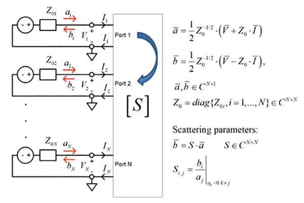
Figure 1. Interconnect system as a multiport.
The Harringon's concept of "loaded scatterers" allows us to turn any interconnect system (even malfunctioning as an antenna) into a multiport and describe it with the waves and scattering parameters, as in Figure 1. Furthermore, the choice of real Zo for all ports makes those waves the "power waves." Now we can define the powers in the balance of power equation through the multiport waves a and b as follows:
P_in is power delivered into the interconnect by transmitter: P_in = |a1|^2 [Wt], |a1| is magnitude of the incident wave at the transmitter end or port 1;
P_out is power delivered to the receiver: P_out = |b2|^2 [Wt], |b2| is magnitude of the transmitted wave at the receiver end port 2 assuming that |a1| != 0 and no incident waves on the other ports |ak| = 0 for all k != 1;
P_absorbed is power absorbed or dissipated by dielectrics and conductors and possibly by absorbing boundary conditions in interconnect models (more on that below);
P_reflected is power reflected back to the transmitter: P_reflected = |b1|^2 [Wt], |b1| is magnitude of reflected wave at the transmitter end, assuming that no incident waves on the other ports|ak|=0 for all k != 1;
P_leaked is power leaked into the other coupled interconnects, modes and, possibly, into power distribution network (PDN – another type of interconnects) and into free space (radiated): P_leaked = sum(|bk|^2 [Wt], k != 1,2; |bk| are waves transmitted to the ports of the coupled interconnects, |ak| = 0 for all k != 1;
P_coupled is power gained from the other coupled interconnects, modes, PDN and free space: P_coupled = |b1|^2+|b2|^2 [Wt], a1 = 0, a2 = 0, ak != 0 for all other k;
FIGURE 2 is a summary for defining elements in the interconnect balance of power. Let's examine those terms further. First, let's assume that the link is localized somehow – no coupling or P_leaked = P_coupled = 0 (the coupling will be a subject for another article). It is hard to do it for the real life "open waveguiding systems" such as a printed circuit board or packaging interconnects, but is close to reality for properly designed interconnect systems. The remaining balance of power is:
P_out = P_in - P_absorbed - P_reflected
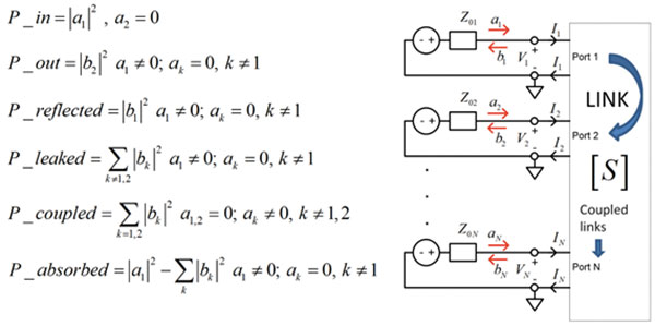
Figure 2. Definition of elements in the interconnect balance of power.
What can we learn from this simple expression? P_out characterizes the transmitted signal and includes signal distortions from absorption or dissipation2 as well as from all kinds of reflections. This is important to know. If more power is reflected or absorbed, then less power is delivered to the receiver – and that means more signal degradation or distortion. It is a little more complicated with the complex termination impedances. So, let's stay with the real termination impedances; it is not a simplification or approximation because all reactive parts of the termination impedance can be easily embedded into S-parameters – the "black box" can take everything in.
P_out can be expressed as insertion loss (IL, a positive number) in dB as:
IL = 10*log(P_in/P_out) [dB]
This is by definition. We can rewrite it with the magnitudes of the multiport waves as:
IL = 10*log(|a1|^2/|b2|^2) = 20*log(|a1|/|b2|) = -20*log(|b2|/|a1|) = -20*log(|S21|)
S21 is the transmission parameter – transmission from port 1 to port 2. The insertion loss is just negative magnitude of the transmission parameter S21 in dB.
P_absorbed characterizes all power losses to heat the materials (the inevitable contribution to the increase of entropy) or dissipated by absorbing boundary conditions in interconnect models. It can be expressed as (no coupling):
P_absorbed = P_in – P_out – P_reflected = |a1|^2 - |b2|^2 - |b1|^2 [Wt]
This is a useful formula in case you want to evaluate the absorbed or leaked (if leaks are modeled with the absorbing boundary conditions for instance).
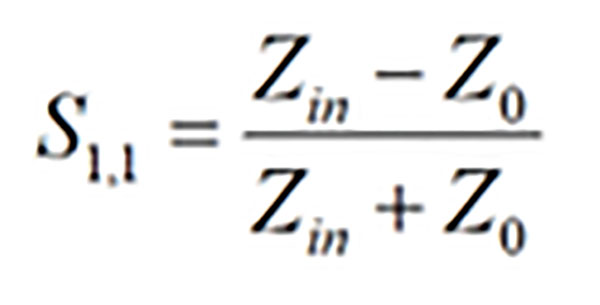
P_reflected characterizes just the reflections and can be expressed as the return loss (RL, a positive number) in dB as:
RL = 10*log(P_in/P_reflected) [dB]
Again, this is by definition. We can also rewrite it with the magnitudes of the multiport waves as:
RL = 10*log(|a1|^2/|b1|^2) = 20*log(|a1|/|b1|) = -20*log(|b1|/|a1|) -20*log(|S11|)
Here S11 is the reflection parameter – reflection at port 1. The return loss is just the negative magnitude of the reflection parameter S11 in dB.
FIGURE 3 shows the expressions for insertion and reflection loss through power:
The absorption or dissipation losses in dielectrics and conductors were discussed in Shlepnev.2 Such losses are inevitable, but can be effectively mitigated at the stackup planning stage – the selection of dielectric and conductor materials and stackup geometry defines the maximal possible communication distance for a particular data rate and power required to transmit the signal.
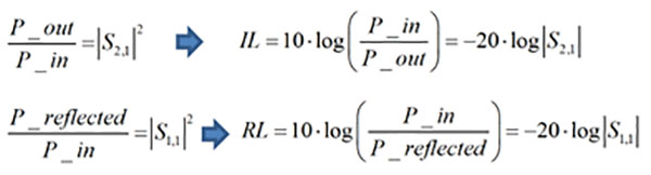
Figure 3. Expressions for insertion and reflection loss through power.
Considering the reflections, they can be further separated into the following categories:
- Reflections from mismatch of transmission line impedance and terminations3
- Reflections from single discontinuities – transitions, vias, AC caps, length compensation structures, gaps in reference plane, ...
- Reflections from periodic discontinuities – fencing vias and cut outs, fiber-weave effect....
Item 1 is discussed in Shlepnev.3 The most important thing for understanding the reflection from that is the formula for reflection parameter from a segment of transmission line with complex propagation constant (Gamma), characteristic impedance (Zc) and length (l) terminated with Zo:

The reflection reaches the maximal values at frequencies where the transmission line length is the quarter of wavelength in line (Lambda) or Lambda/4+n*Lambda/2 in line (see definitions in Shlepnev3):
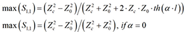
Here alpha is the attenuation constant that increases with the frequency.2 This is another remarkable formula – the reflections are smaller for lines with more losses (greater alpha) and at higher frequencies.3 The last part is valid only if there are no discontinuities. It makes everything perfectly clear with the choice of characteristic impedance: the closer Zc to the termination impedance Zo, the lower the reflections. A link with Zc=Zo would be the best link, if it were possible to design and build it like that. What prevent us from doing it are all kinds of transitions. In reality, just some parts of interconnects look like, and can be modeled as, the transmission lines. There are also transitions between the transmission lines: packages, connectors, vias, length compensation structures, AC coupling capacitors, transitions between the transmission lines of different types or with different cross-sections. Accurate analysis of a complete link with the discontinuities usually requires validated software with 3-D electromagnetic analysis capabilities. Before providing examples of such numerical analysis, let's write a couple of practical formulas for qualitative and quantitative analysis of the reflections from the discontinuities. The first formula is for the input impedance of a transmission line segment loaded with ZL impedance (FIGURE 4).
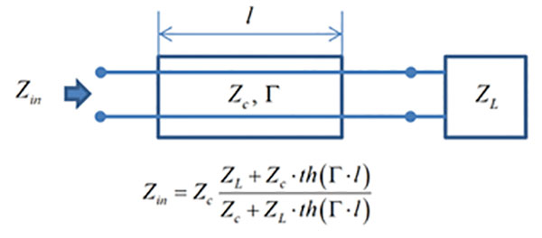
Figure 4. Input impedance of a transmission line segment loaded with ZL impedance.
It can be easily derived starting with the exponential expansion3 by setting the boundary conditions on the right side. The formula for the impedance can be used recursively starting from the receiver by including discontinuities in a transmission line that have expressions for the impedance – capacitances, inductances or combinations, stubs and so on. All you need to know is how to connect the complex impedances in parallel and in series. As soon as we know the input impedance of the link at the transmitter side, the reflection parameter can be computed as:
Note that this is exactly the value as the reflection coefficient that is usually designated with Gamma.4 There are no differences in this context. The formula can be also inverted, to compute Zin from the reflection parameter.
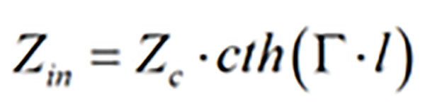
Now, let's examine a few cases. First, if ZL = Zc then Zin = Zc and the reflection parameter is S11=(Zc-Zo)/(Zc+Zo) – this is reflection from the ideally terminated transmission line segment or from the infinite transmission line. It correlates well with the S11 provided earlier for the transmission line segment with the infinite length (cth is the unit in this case). Another limit case is ZL=infinity – this is open-circuited segment of transmission line. In this case Zin is particularly simple:
What can we learn from that in the context of interconnects? It can be used to model and explain the effect of stubs. The first order approximation for a via-hole discontinuity is a transmission line model. If via is going through all stackup layers, but connects only one surface layer with an interior layer for instance, the remaining part of the via is a stub connected in parallel to the link. If stub length is a quarter of wavelength in corresponding equivalent transmission line model, we have input impedance of the stub as follows:
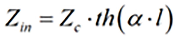
It is zero if alpha or attenuation is zero; that means it short-circuits the link. With zero Zin, the reflection is S11 = -1. It does not matter what the other parts of the link look like. Never let it happen at the frequencies close to the Nyquist frequency! So, it is all the transmission line trigonometry – though hyperbolic in this case, literally.
After having some fun with the formulas and the limit cases, let's analyze a couple of ideal discontinuities. The analysis can be done with the formulas as well (a good exercise), but it is much easier to do it with the software – Simbeor in this case. A 0.1pF capacitor connected in parallel into a segment of an ideal 50Ω transmission line (yes, ideal transmission lines exist in the software as well) will have magnitude of reflection (left graph, left axis, red line) and phase of reflection (left graph, right axis, brown line), as shown in FIGURE 5.
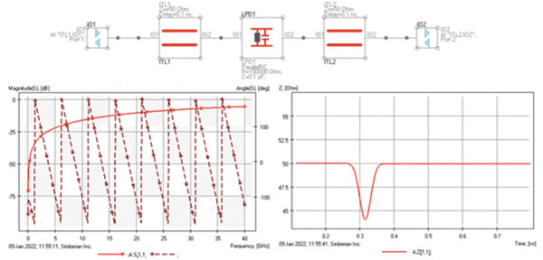
Figure 5. A 0.1pF capacitor connected in parallel into segment of ideal 50Ω transmission line showing magnitude of reflection (left graph, left axis, red line) and phase of reflection (left graph, right axis, brown line)
Time-domain reflectometry (TDR) is also shown on the right plot. It is much easier to recognize the capacitance on the TDR plot as the "capacitive" dip. The TDR is computed here directly from the frequency-domain response with 40ps Gaussian step function.
Next, let's look at 0.25nH inductance connected in series into the same ideal 50Ω transmission line segment shown in FIGURE 6. The frequency-domain reflection magnitude shown in blue on the left graph is exactly as the reflection from the capacitance (the values are intentionally selected to have it like that). However, the phase is different (though it is difficult to conclude something from it) and the TDR shows a clear "inductive" bump.
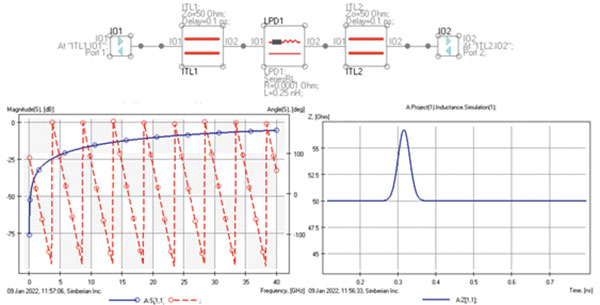
Figure 6. 0.25nH inductance connected in series into the same ideal 50Ω transmission line segment.
What if we combine 0.1pF capacitance and 0.25nH inductance as a C/2-L-C/2 circuit? The reflection will go down, as shown in FIGURE 7. That explains how the transmission line works: t-line has both capacitance and inductance with the ratio equal to the characteristic impedance; Zo = sqrt(L/C) = 50Ω, as in this case. The reflections in the frequency domain are small, but not zero. This is because of the model uses lumped L and C in the middle of continuous transmission line segment and it behaves as the t-line only at lower frequencies. A TDR with a 40ps rise time is almost flat, however, and does not resolve such lumped discontinuity in this case.
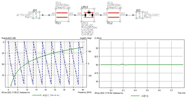
Figure 7. 0.1pF capacitance and 0.25nH inductance combined as C/2-L-C/2 circuit.
Finally, we show a few practical examples of the electromagnetic discontinuity analysis with validation as used in our DesignCon 2020 tutorial.5 The first example is the capacitive via from CMP-28 validation platform designed by Wild River Technology (FIGURE 8).
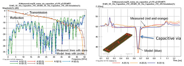
Figure 8. Capacitive via from the CMP-28 validation platform.
Modeled and measured magnitudes of the transmission and reflection parameters are shown on the left graph and corresponding TDRs are on the right. The link includes coaxial connectors and launches (inductive bumps at the beginning and end). The reflections in this case are not show-stoppers: the link is short and the added capacitance is not so big. It was intentionally capacitive. (More analysis to measurement correlation examples from the CMP-28 platform are in Shlepnev.6)
Another two practical examples with the analysis to measurement correlation are from the EvR-1 project7 (see also app notes #2018_01, 2018_07 and webinar #8 at simberian.com). FIGURE 9 shows the modeled and measured magnitudes of the differential reflection and transmission parameters and differential and common-mode TDRs for a differential link with two vias from BOTTOM to INNTER6 layers with stubs (structure EvR1-C1).
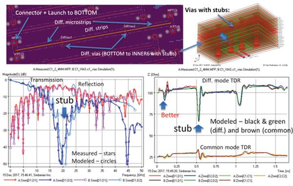
Figure 9. Modeled and measured magnitudes of the differential reflection and transmission parameters and differential and common-mode TDRs for a differential link with two vias from BOTTOM to INNTER6 layers with stubs.
The via stubs almost short-circuited the link at about 20GHz; the reflection parameter (reddish lines with circles) went up and the transmission parameters (bluish lines with stars) went down around the stub resonance frequency. With the transmission below -30dB, the signal harmonics at those frequencies will not go through. Corresponding differential TDR shows a large capacitive dip at the via location, although it is difficult to conclude from TDR at which frequency the via would destroy the signal. Note that the correlation between the model and measurements is as good as it usually gets; this is because of the "sink or swim" approach used in Marin and Shlepnev.7
What can be done to avoid such harmful reflections? Via back-drilling and optimization – below is structure EvR1-C2 with the back-drilled and optimized vias for the transition between the same layers (FIGURE 10).
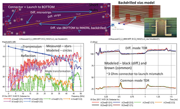
Figure 10. EvR1-C2 with back-drilled and optimized vias for the transition between the same layers.
The reflection is below -10dB up to 30GHz and no bumps at the location of the vias – the link is as good as it can be for all practical purpose. Note that the correlation of smaller reflections is more difficult to achieve because of the manufacturing variations that were also investigated for this particular board in Marin and Shlepnev.7
The bottom line is that reflections – even from a single discontinuity – can destroy your signal, although the effect of major discontinuities can be predicted with validated models before the board design (pre-layout analysis) and must be predicted after the board is designed and before it goes into manufacturing (post-layout analysis). Examples of discontinuity analysis and optimization for typical PCB links with Simbeor electromagnetic signal integrity software are provided in the demo-video section at simberian.com/ScreenCasts.php?view=list. •
References
1. Y. Shlepnev, "How Interconnects Work: Bandwidth for Modeling and Measurements," Simberian App Note #2021_09, Nov. 8, 2021.
2. Y. Shlepnev, "How Interconnects Work: Absorption, Dissipation and Dispersion," Simberian App Note #2021_10, Nov. 26, 2021.
3. Y. Shlepnev, "How Interconnects Work: Impedance and Reflections," Simberian App Note #2021_1, Dec. 22, 2021.
4. Wikipedia, Reflection of Signal on Conducting Lines, https://en.wikipedia.org/wiki/Reflections_of_signals_on_conducting_lines.
5. Y. Shlepnev and V. Heyfitch, "Design Insights from Electromagnetic Analysis & Measurements of PCB & Packaging Interconnects Operating at 6- to 112-Gbps & Beyond," DesignCon 2020 Proceedings, January 2020.
6. Y. Shlepnev, "Guide to CMP-28/32 Simbeor Kit," CMP-28 Rev. 4, September 2014.
7. M. Marin and Y. Shlepnev, "40 GHz PCB Interconnect Validation: Expectation vs. Reality," DesignCon 2018 Proceedings, January 2018.
Ed: To review figures showing 1) the interconnect balance of power expressed through S-parameters and 2) insertion loss, return loss, coupling and leaks, see the Appendix in the online or digital version.
Yuriy Shlepnev is president and founder of Simberian (simberian.com), where he develops Simbeor electromagnetic signal integrity software. He has a master's in radio engineering from Novosibirsk State Technical University and a Ph.D. in computational electromagnetics from Siberian State University of Telecommunications and Informatics. He was the principal developer of electromagnetic simulator for Eagleware and a leading developer of electromagnetic software for the simulation of signal and power distribution networks at Mentor Graphics. His research has been published in multiple papers and conference proceedings; This email address is being protected from spambots. You need JavaScript enabled to view it..


