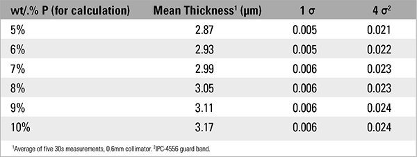
The actual phosphorus content in the deposit must be considered.
While the current focus in the electronics industry is chips, components and microelectronics, the printed wiring board (PWB) also plays a vital role. Continued miniaturization and environmental considerations, such Restriction of Hazardous Substances Directives (RoHS), have led the industry to create and improve surface finishes to meet current and future generations of electronic assemblies. Two PWB finishes have become very common: ENIG and ENEPIG. The industry trade association, IPC, released IPC-4552 in 20021 to help standardize the global printed circuit board industry around a specification for ENIG. IPC-4556 was released in 20132 to establish industry standards around ENEPIG surface finishes.
The electroless nickel layer plays important roles in the functionality of printed boards. Electroless nickel provides a diffusion barrier between the copper basis metal and the surface finish layers of immersion gold (ENIG) or electroless palladium and gold (ENEPIG). It also provides a stable metallization for wire bonding, and acts as a wear resistant layer for switch pad applications that copper, or other copper basis surface finishes, cannot offer. The formation of nickel-tin (Ni3Sn4) intermetallic compounds (IMCs) have shown to offer similar long-term reliability when compared to copper-tin IMCs (Cu6Sn5 and Cu3Sn) that have been the standard for reliability studies since the inception of the electronics industry.3 Both IPC-4552B and IPC-4556 specify the electroless nickel thickness for rigid boards shall be 3 to 6µm (118.1 to 236.2µin).4,5 IPC-4556 contains an additional requirement to apply a ±4 Sigma (four standard deviations) from the mean to account for measurement uncertainty. (Note: IPC-4552 also provides electroless nickel thickness requirements for flexible circuits. For brevity, this article addresses only rigid boards. The concepts detailed can be applied to flex boards, however.)
The background for the thickness range requirements for electroless nickel arise from both practical and physical requirements. IPC-4552B indicates electroless nickel thicknesses below 3µm may be appropriate for high-frequency applications.6 Electroless nickel thicknesses below 1.27µm (50µin), however, are not recommended due to increased potential for copper diffusion through the electroless nickel layer.7 Practically, the time to deposit 1.27µm of electroless nickel is shorter than the time to deposit the required thicknesses of immersion gold, especially important on an automated plating line. Plating the minimum 1.27µm would require freshly deposited nickel PWBs to be placed into a "holding station" or rinse water tank for an extended period. This risks passivation of the nickel prior to the immersion gold (or palladium) deposit. Passivated nickel presents problems with subsequent plating layer(s) adhesion and solderability. To minimize hold times, and potential impact on the nickel, the minimum thickness has been established at 3µm. This was found to work well with automated plating lines as well as providing an excellent minimum thickness for wire bonding. The maximum thickness of 6µm (236.2µin) was incorporated to prevent high insertion forces and therefore possible damage for press-fit pins into PWB through-holes.8
X-ray fluorescence (XRF) instrumentation is the only accepted IPC-4552B metrology method9 to measure thicknesses for plated layers. IPC-4556 does not restrict ENEPIG thickness measurements to XRF but Appendices 4 and 9 highlight and detail specific guidance and considerations for use of XRF to measure ENEPIG.10 XRF instruments calculate thicknesses by determining the amount of mass of material present in a defined measurement area. The analysis, or measurement, area of a specific XRF measurement is colloquially known as the "spot size." The spot size is defined by type of XRF system used, either with mechanical collimators or polycapillary optics. IPC-4552B specifies use of either a 0.3mm or 0.6mm mechanical collimator, or a system equipped with polycapillary optics (measurements made with polycapillary optics shall be made with a scan over the surface).11 IPC-4556 does not directly specify a spot size but does detail measurement spot size "shall not exceed 30% of the feature size being measured."12
Calculation of coating thickness, using XRF, while complicated, can be simplified to a core principle, measuring the amount of mass of material within in a known measurement surface area. The measurement surface area is defined by either the collimator size or polycapillary optic spot size. An XRF instrument observes and quantifies an amount of mass of material(s), uses known or user input for the density of the material(s), and calculates a thickness value.
Thus, calculating the thickness of electroless nickel presents challenges. Electroless nickel is a self-sustaining, autocatalytic reduction process using hypophosphite chemistry.13 As the nickel deposits on a substrate, by design, a quantity of phosphorus is incorporated within the nickel layer. The addition of phosphorus changes the density of the deposit. As described in the paragraph above, XRF measurements use mass in a defined surface area to derive a layer thickness. Changes in density, if not included in the measurement calculation, will present themselves as a change in layer thickness.
Accurate measurement of the electroless nickel layer thickness is possible if a user corrects for density changes caused by the inclusion of phosphorus in the nickel deposit in a specific sample. The thickness measurement will be calculated with the appropriate density (e.g., fixed percentage; 92% Ni, 8% P) of the specific sample. Some XRF instruments are capable of directly measuring the phosphorus content (calculating the alloy percentage in wt.%) in each sample and will automatically calculate a thickness with the correct density.
Experimental
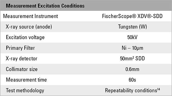
Testing for the effects of phosphorus content on the thickness was conducted on a ENIG calibration standard, serial identifier AVPQ (TABLE 1). The sample was measured using a calibrated XRF instrument with collimated optics and measured with the test conditions as detailed in TABLE 2.
TABLE 1. Measurement Sample
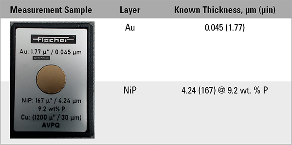
TABLE 2. Sample Test Conditions
The sample was measured five times under repeatability conditions14 (same person, same location, short time frame, same instrument, etc.). The phosphorus content was initially set at 5% and the measurement calculation recipe was then manually adjusted (FIGURE 1) between each group of measurements, in increments of 1%, to a final value of 13 wt.% P. Mean values and standard deviations were calculated from the individual measurements (TABLE 3). The calculated thickness was plotted vs. the wt.% P used in the measurement calculation (FIGURE 2).
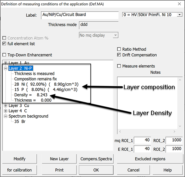
Figure 1. Setting the phosphorus % in the measurement recipe.
Table 3. Measurement Data, Sample AVPG, Changing wt.% P
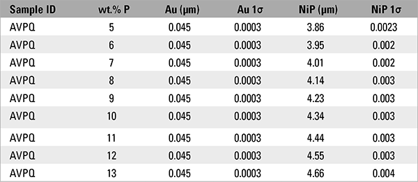

Figure 2. Electroless nickel layer thickness vs. wt.% P content.
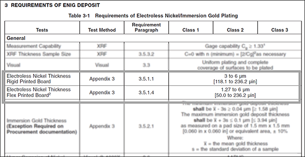
Figure 3. IPC-4552B thickness specification for ENIG.15
Additional testing was performed on a second sample to evaluate how different percentages of phosphorus affected electroless nickel thickness measurements near the lower limit of the IPC specifications. Testing was performed using a certified electroless nickel sample at 3.05µm (120.1µin) containing 8% phosphorus over a solid copper base. The phosphorus content for the thickness calculation was manually varied, in the measurement settings (Figure 1), from 5 to 10 wt.% P. These data are displayed in TABLE 4.
Table 4. Electroless Nickel Thickness on Copper with Varying wt.% P
Discussion
The effects of phosphorus content on electroless nickel are apparent from the data shown in Tables 3 and 4 and graphically represented in Figure 2. The data clearly show the effects changing phosphorus content has on the layer thickness of an electroless nickel deposit. This explains why the actual phosphorus content in the deposit must be considered by both PWB manufacturers and end-users when evaluating electroless nickel thickness vs. the IPC specifications. This becomes most relevant when parts are subject to either acceptance or rejection based on the nickel layer thickness.
The risk of rejecting good parts, or conversely accepting failing parts, is real if we accept or reject solely on the thickness of the electroless nickel layer. Recall from Figure 2 and Table 3, the dimensional thickness of the electroless nickel layer is affected by phosphorus content in the layer. From Table 4 we see how an understanding of these effects is critical when the sample is at, or near, the specification's tolerance (Figures 3 and 4). Referring to Table 4, the sample, as measured at 8% phosphorus, will pass both IPC-4552B and IPC-4556 minimum electroless nickel thickness, but will fail if the sample is measured at 7% phosphorus.

Figure 4. IPC-4556 thickness specification for ENEPIG.16
The potential for false rejection or acceptance increases when we look at ENEPIG and IPC-4556. As mentioned, from Figure 4, with ENEPIG the standard deviation of the electroless nickel measurements must also be considered. FIGURE 5 shows a plot of 300 randomly generated data points. In this case, using the measurement standard deviation (1σ) of 0.005µm from Table 4, the part must measure a minimum of 3.02µm to meet a minimum thickness of 3µm ±4σ.
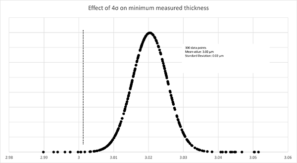
Figure 5. ENEPIG ±4σ consideration on lower EN limit specification.
Conclusion
Both IPC-4552 and IPC-4556 are important industry standards for the manufacturing of reliable electronic assemblies. Much of the attention in printed wiring boards is paid to the precious metals. The electroless nickel layer is also important, for reasons of solderability, shelf life, durability, and dimensional requirements for press fit pins.
Both IPC specifications apply a 3-6µm [118.1-236.2µin] thickness specification to the electroless nickel layer. This creates potential problems for both the PWB fabricator and the end-user; there may be false rejections or acceptance because an incorrect phosphorus content was used to calculate the thickness. This potential thickness measurement error is most relevant for parts with electroless nickel thickness at, or very close to the minimum or maximum tolerances.
Care should be taken to use the correct phosphorus content for the sample being measured or use XRF instrumentation capable of directly evaluating the wt.% P in the sample being measured.
References
1. IPC-4552B, Specification for Electroless Nickel/Immersion Gold (ENIG) Plating for Printed Boards, 2021.
2. IPC-4556, Specification for Electroless Nickel/Electroless Palladium/Immersion Gold (ENEPIG) for Plating Printed Circuit Boards, 2013.
3. C. C. Lee, P. J. Wang and J. S. Kim, "Are Intermetallics in Solder Joints Really Brittle?" 2007 Proceedings 57th Electronic Components and Technology Conference, 2007, doi: 10.1109/ECTC.2007.373866.
4. IPC-4552B, Specification for Electroless Nickel/Immersion Gold (ENIG) Plating for Printed Boards, 2021.
5. IPC-4556, Specification for Electroless Nickel/Electroless Palladium/Immersion Gold (ENEPIG) for Plating Printed Circuit Boards, 2013.
6. IPC-4552B, Specification for Electroless Nickel/Immersion Gold (ENIG) Plating for Printed Boards, 2021.
7. Ibid.
8. Gerard O'Brien interview, conducted by Robert Weber, Sept. 15, 2022.
9. IPC-4552B, Specification for Electroless Nickel/Immersion Gold (ENIG) Plating for Printed Boards, 2021.
10. IPC-4556, Specification for Electroless Nickel/Electroless Palladium/Immersion Gold (ENEPIG) for Plating Printed Circuit Boards, 2013.
11. IPC-4552B, Specification for Electroless Nickel/Immersion Gold (ENIG) Plating for Printed Boards, 2021.
12. IPC-4556, Specification for Electroless Nickel/Electroless Palladium/Immersion Gold (ENEPIG) for Plating Printed Circuit Boards, 2013.
13. Ibid.
14. International Organization for Standardization, ISO 5725-1:1994, Accuracy (Trueness and Precision) of Measurement Methods and Results – Part 1: General Principles and Definitions.
15. IPC-4552B, Specification for Electroless Nickel/Immersion Gold (ENIG) Plating for Printed Boards, 2021, p. 6.
16. IPC-4556, Specification for Electroless Nickel/Electroless Palladium/Immersion Gold (ENEPIG) for Plating Printed Circuit Boards, 2013, p. 4.
Ed: This article is adapted from a paper of the same title first presented at the IPC Apex Expo Technical Conference in January 2023, with original work published within conference proceedings.
Robert Weber is technical director of Fischer Technology (fischer-technology.com); This email address is being protected from spambots. You need JavaScript enabled to view it..
PCB East, the electronics industry trade show for the East Coast! Coming May 9-12, 2023


