A study of the influence of design parameters that impact success.
A microvia is defined in IPC-T-50M as “a blind structure (as plated) with a maximum aspect ratio of 1:1 when measured in accordance with FIGURE 1, terminating on or penetrating a target land, with a total depth (X) of no more than 0.25mm [0.00984 in] measured from the structure’s capture land foil to the target land.”
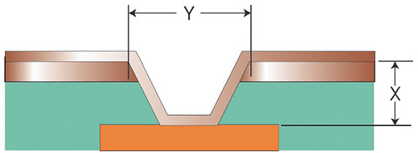
Figure 1. Microvia definition per IPC-T-50M. (Note: X/Y = microvia plating aspect ratio, with X < 0.25mm (0.00984") and aspect ratio < 1:1.)
Advantages to using microvias in PCB design include but are not limited to signal integrity, routing real estate, and pin escape. The most common reason that drives designs to use microvias is the need to escape the pins of a fine-pitch part. As pin pitch on an integrated circuit (IC) is reduced, the design starts to approach a threshold where mechanically drilled vias are not possible. When this happens, other routing solutions such as microvias are required. Use of area array components with a pitch of less than 0.8mm will very likely require the use of microvias to escape the pins of the component, and these components are becoming common in high-reliability electronics such as space hardware and military/defense products. Another advantage is microvias can be used to make connections between two adjacent layers, thus saving a significant amount of routing real estate by not requiring a via that spans multiple layers as a mechanically drilled via typically would. And microvias help with signal integrity of high-speed digital or radio frequency (RF) circuits. At higher frequencies designs can be very sensitive to signal reflection caused by via stubs, and microvias may be required to mitigate signal integrity issues.
Once it is determined microvias are necessary, many design decisions remain to be made. On the lower complexity end of the spectrum the design may require only one layer of microvias spanning from the outer layer to the next layer in. On the other end of the spectrum the design may require microvia structures spanning every layer, also known as Every Layer Interconnect (ELIC) or All Layer Via (ALV). While it would be very difficult to capture the entire design spectrum, the more common design parameters for current aerospace designs were tested and the next section covers those design details.
Coupon/Panel Design
A 12" x 18" panel of test coupons was designed to test and examine various microvia structures. Conductor Analysis Technologies (CAT) has a web-based interface for coupon generation1 to simplify the creation process; however, this panel was designed by hand, leveraging a previous design created by a coworker. The design calls out polyimide per IPC-4101/40, /41 or /42, currently the most common requirement for our designs. In the future other material may be explored, but for now all panels were built using polyimide. The panel contains 54 D-coupons, 37 coupons with isolated via structures for cross-sectional evaluation (similar to IPC A/B coupons and, for simplicity’s sake, they will be referred to here as A/B coupons) and two peel strength coupons, with embedded microvias, to be used as test strips. FIGURE 2 shows the test panel design.
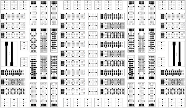
Figure 2. Panel design.
Each D-coupon contains two daisy chains of vias with plated through-hole (PTH) connections on each end of the chain. A press-fit header is assembled onto the coupon, which enables a Kelvin (or 4-wire) resistance measurement to be taken, for precise resistance measurement of the chain. Each coupon in the design represents different variations of microvia size and pitch. Most daisy chains consist of the transition between two different via spans (e.g., 1-2 and 2-3); however, a few daisy chains utilize almost all via spans and the daisy chain traverses the top to the bottom of the board (the 3-4 microvia is the only via span left out of these daisy chains). The size and pitch remain constant within each daisy chain, and through the numerous D coupons on the panel, many variations may be examined.
The goal was to straddle microvia diameters and aspect ratios representative of current design practices, but to also use design parameters that start to push the limits of what is considered good design practice. Microvias of 5, 6 and 7 mil diameter were used (to be clear, this is the diameter of the laser-formed microvia at the capture pad), and all microvias were copper-filled. The design supports a constant dielectric thickness (approximately 3.8 mils), which means multiple aspect ratios can be examined by altering the microvia diameter alone. A 3.8-mil dielectric plus 0.5oz. foil is about 4.5 mils thick, and for a 5, 6 and 7 mil microvia this yields aspect ratios of 0.90:1, 0.75:1 and 0.64:1, respectively.
Microvia structure pitch was varied between 0 and 20 mils, in increments of 5 mils. Note the pitch between vias is measured center to center, so a via that has a 0-mil pitch to another in the vertical plane can also be referred to as a stacked via structure. The microvia pad size used was 14 mils, so microvia transitions on a 5- or 10-mil pitch will have overlapping pads; at a 15-mil pitch the pads are no longer overlapping.
FIGURE 3 illustrates the transition between the 1-2 and 2-3 vias in the bottom chain (15 mils in this case), and the top chain shows the transition between one staggered structure pair to the next. Each of the two chains are on the same grid (50 mils), with just over 100 via transitions per chain. Several coupons have a larger grid pitch (150 mils), however, meaning the number of via structures and transitions in the chain is reduced. The purpose of this was to determine if the number of structures in the chain had a major impact on resistance variation of the chain during testing. If each structure contributes a resistance delta to the overall measurement, the theory is that more vias in the chain would increase the probability of failure. The more transitions, the greater the resistance delta between each thermal cycle, thus making it more difficult to meet the 5% resistance change threshold required by IPC-TM-650 method 2.6.27B.2 The theory and the data did not correlate: all the coupons on a 150-mil grid passed thermal stress testing as did all their counterparts on a 50-mil grid.
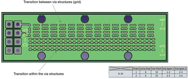
FIGURE 3. Layer 2 of a representative D coupon.
When using D-coupons for acceptance testing, it is important the coupon be designed properly by ensuring the via structures are the same as in the board design. If designed properly and tested to IPC-TM-650 method 2.6.27B, the D-coupon is an excellent tool for testing the robustness of the via structures to withstand the thermodynamic effects caused by convection reflow assembly. The D-coupons are ideal for via reliability testing because they can represent a variety of propagated via structures and transitions, the same as the board design. The electrical resistance of the via structures is monitored while undergoing a representative reflow profile, which is the harshest environment the PCB will see in its lifetime and when plating separation is most likely to originate.
Panel Fabrication
Two PCB fabricators were selected as partners on this effort, henceforth referred to as Fabricator A and Fabricator B. Early in the project, each fabricator supplied input on the design to ensure all interested design parameters were captured. A statement of work was created for each fabricator to flow requirements that deviated from standard build requirements such as:
- Pulling coupons from the panel after certain steps in the fabrication process
- Recording chemical bath analysis results
- Supplying monthly results for tensile strength, elongation and purity testing
- Adding a TMA coupon for Tg testing of the base material.
These data were collected to aid in failure analysis or process investigation, if needed.
Two panels of coupons were procured from each fabricator. Fabricator A had several D-coupons fail during electrical testing per IPC-9252B, which is part of the standard performance specification testing PCBs are subject to for lot acceptance. Due to these failures they had to fabricate third and fourth panels. Between the four panels fabricated, they shipped us all D-coupons that passed electrical test. Some coupon positions yielded 0%, and some yielded 100% from all four panels. The total number of D-coupons delivered was 152 of 216 (54 D-coupons per panel x four panels). Fabricator B had to scrap panels 1 and 2 in their entirety, due to a material stackup issue, but were able to ship 108 of 108 D-coupons from panels 3 and 4.
Coupon Testing
D-coupons were sent to Conductor Analysis Technologies for thermal stress and thermal shock testing as outlined below. CAT tested 108 coupons from each fabricator. Since Fabricator A delivered more than 108, the coupons were sorted and prioritized, starting with coupons containing the smaller diameter and tighter pitch between the transition.
Convection reflow assembly simulation. Thermal stress testing simulates thermodynamic effects caused by the assembly process, specifically the reflow process, which is the harshest environment the PCB will experience and when microvia cracking is most likely to originate. Test method 2.6.27B is referenced in the special requirements section (3.10) of IPC-6012E3, and is a required conformance test for any PCB containing microvias built to the Space and Military Avionics Applications Addendum (IPC-6012ES).4 Testing was performed on a D-coupon, as previously described. Both tests described in this section require D-coupons to be baked for moisture removal for a minimum of 6 hr. at 105° to 125°C. The D-coupon is then thermally stressed through a representative reflow profile simulation, with upper and lower limits defined in the test method. FIGURE 4 shows the upper (red) and lower (blue) limits for the 260°C reflow profile. The test method also defines 230° and 245°C reflow profiles. The intent of the multiple reflow profiles is to give the end-user options to test with a reflow profile that is representative of what the deliverable boards will be subjected to during assembly. Most products built at the authors’ company will experience a tin-lead reflow profile with a peak temperature near 230°C. Hand assembly and rework are very common processes, however, and these temperatures are very difficult to account for when trying to simulate the entire assembly process of a PCB. While we may not be able to encompass all assembly processes the PCB may be subjected to, testing to the higher 260°C reflow temperature profile provides additional margin to give confidence the PCBs will also survive a reasonable level of hand assembly or rework processes.
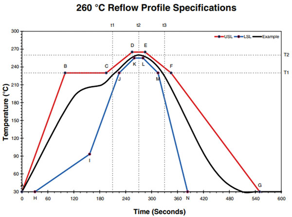
Figure 4. Example of IPC-defined limits for a reflow profile (IPC-TM-650, method 2.6.27B).
The IPC test method requires the resistance of the daisy chain be continuously monitored during the entire reflow cycle and consists of at least one reading per sample net every second while the coupons are thermal-cycled. The minimum number of required thermal cycles is six, but for this effort the coupons were subjected to 12 cycles to gather additional data beyond the minimum requirement. Pass/fail criteria are based on a resistance change in the daisy chain. The maximum resistance during the first cycle is used as the reference (baseline) resistance for the test. During thermal cycling the resistance shall not exceed a 5% change from the baseline measurement. FIGURE 5 shows results from 24 D-coupons tested for 12 cycles at the 260°C reflow profile. One chain stands out because the resistance increases each cycle and never returns to the original resistance value even at ambient temperature; this is an obvious failure. A few chains get progressively worse each thermal cycle, with some exceeding the 5% pass/fail criteria indicated by the red line. Many maintain near a 0% change in resistance from the first thermal cycle. The lack of resistance changes between each thermal cycle is a good indicator that the harsh environment of the reflow profile has not adversely affected the connectivity of the microvias.
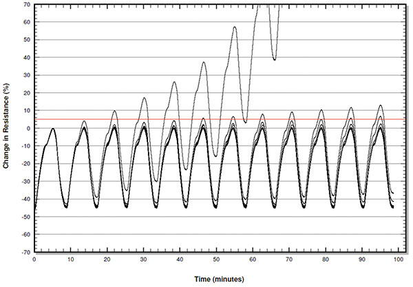
Figure 5. IPC-TM-650, method 2.6.27B results after 12x cycles.
Thermal shock, thermal cycle and continuity. In addition to thermal stress testing, thermal shock testing per IPC-TM-650 method 2.6.7.2C5 was performed on several D-coupons. This testing requires thermal stress testing be performed first, so this test must be performed in tandem with IPC-TM-650 method 2.6.27B. Several coupons that passed thermal stress testing were then subjected to thermal shock testing, which is a more rapid temperature cycle change, for 100 cycles. The test method defines the max. temperature of the thermal cycle to be the least of:
- Material Tg – 10°C (lowest Tg of the materials used in the specimen, but not lower than 125°C)
- Reflow process peak temperature – 25°C
- 210°C.
With peak reflow temperature around 230°C and material with a minimum Tg of 250°C (per the datasheet), the max thermal cycle temperature is derived from the second bullet above and is 205°C. The default of -55°C was used for the low end of the temperature cycle. Resistance readings are recorded once per cycle, with cycle durations of approximately 8 min. and a maximum allowable resistance change of 5% after 100 cycles. FIGURE 6 shows the results of 24 nets from Supplier A: Some nets maintain a relatively constant resistance throughout the test, and some have a steady increase in resistance throughout the cycling.
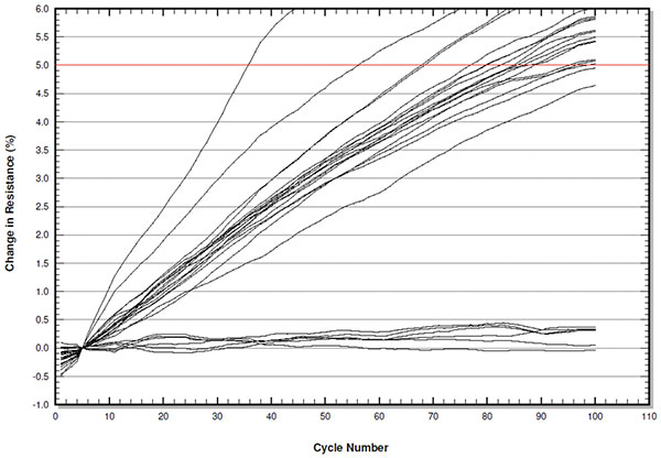
Figure 6. IPC-TM-650, method 2.6.7.2C results after 100x cycles.
Discussion
Fabricator B testing yielded almost 100%, and because of that, this discussion will focus on the data from the testing of coupons from Fabricator A. FIGURES 7 and 8 show the yield comparison of three types of electrical testing that took place; the two methods mentioned above and electrical testing per IPC-9252B. TABLES 1 and 2 contain the details behind the yield percentages, such as the number of coupons or nets tested.
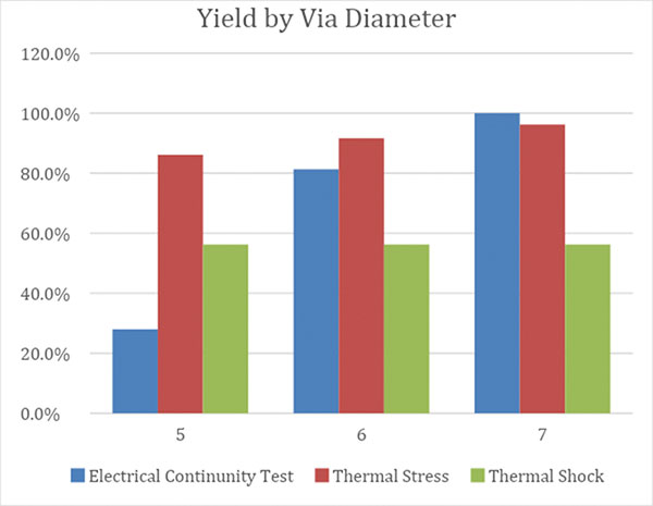
Figure 7. Fabricator A test data organized by via diameter.
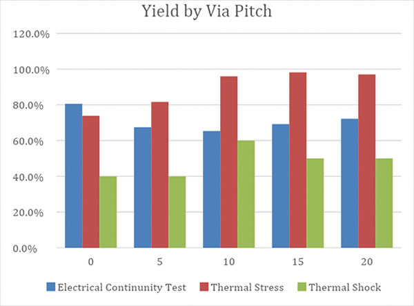
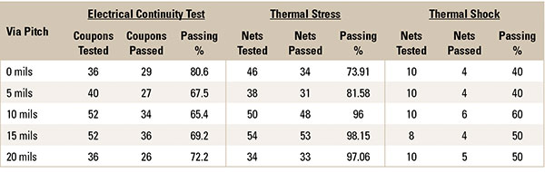
Figure 8. Fabricator A test data organized by via pitch.
Table 1. Testing Results Sorted By Via Diameter
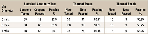
Table 2. Testing Results Sorted By Via Pitch
Electrical testing per IPC-9252B is accomplished by flying probe or bed-of-nails testing and is performed at ambient temperature.6 No temperature cycling is associated with this testing. All coupons that failed electrical testing did so due to opens in the daisy chain. The resistive continuity testing (Figure 7) produced some interesting results: yield increased over 50% when the microvia diameters increased from 5 mils to 6 mils, and at 7 mils yield jumps to 100%. This was the first indicator of the importance of microvia diameter and/or aspect ratio.
Thermal stress testing results also improved as via diameter increased. As mentioned, 5-mil diameter vias had the most failures in electrical testing at ambient. Likewise, coupons with 5-mil diameter microvias had the most failures when subjected to thermal stress testing. Yield increased approximately 5% when diameter was increased to 6 mils, and increased another 5% for the 7-mil microvias, which had a yield of just over 96%.
The final type of testing performed on the coupons was thermal shock testing. The sample size of coupons put through thermal shock testing was limited – only 24 of the 108 coupons from each fabricator were tested – as this testing wasn’t as high priority as thermal stress testing and funding was limited. The environments were much less harsh on the coupons, with the maximum testing temperature 205°C. For that reason, more focus was placed on thermal stress testing, although more data could shed light on the importance of thermal shock testing.
Looking back to Figure 6 (thermal shock testing), a pack of nets show a steady increase in resistance for each subsequent cycle, and several of those nets do not exceed the 5% threshold, meaning those nets passed acceptance testing. The rate of change is alarming but does seem to be leveling. It would be interesting to see if the resistance change does level past 100 cycles, or if these vias could potentially be a reliability risk to hardware, by continuing to increase in resistance each thermal cycle and eventually become an open circuit.
Thermal shock test results sorted by via diameters showed flat results, at 56% across all via diameters. Unfortunately, this doesn’t leave anything conclusive when trying to identify correlating trends with via diameter and thermal shock testing.
Figure 8 sliced the same data by via pitch; the center-to-center distance between staggered vias. The results from electrical testing at ambient were relatively flat, with limited correlation to pitch. The 10-mil pitch yielded the lowest at 65%, whereas the 10-mil pitch had some of the best results through thermal stress and thermal shock testing. Interestingly, the 0-mil (stacked microvias) pitch vias had the highest electrical test yield: 80%. This is a testament that electrical testing cannot be relied on for screening microvia construction integrity.
Thermal stress testing did show an increase in yield with greater via separation. Yields were just under 75% on the stacked vias (0-mil pitch). As pitch increased to 5 mils the yield jumped to just over 80%, and at 10 mils the yield was 96%. The jump in yield between vias on 5-mil pitch and 10-mil pitch is relatively large, a 16% increase. At 5-mil pitch, the holes are tangent, but due to drill misregistration there is a chance the 5-mil holes could have some overlap. At 6 and 7 mils the holes will have some overlap in their nominal locations, but when the pitch is increased to 10 mils there is no overlap of the holes. All microvias have a 14-mil pad, which means when there is a 10-mil pitch between vias there is some overlap of the pads, but when the pitch is increased to 15 mils there is no overlap of the pads. With this limited amount of data, it is difficult to determine if the separation of the microvia holes or pads is more critical. But with a larger jump in yield when the microvia holes are separated versus the separation of pads, the data suggest it is more important to separate the microvia holes, but higher yield can still be achieved by ensuring the microvias are far enough apart that the pads do not overlap.
When the thermal shock data were sorted by via pitch, the results were also inconclusive. It will take more data to understand if there is a trend when it comes to thermal shock testing.
In summary, the component packaging may dictate the diameter and pitch of the via separation required to ensure large enough routing channels to escape from fine-pitch parts with producible line widths and spacing. The thermal stress reflow simulation testing results show higher yields with larger microvia diameters/lower aspect ratios and greater via separation, so it is important to maximize these for higher yields.
Failure Analysis
Several coupons were selected to undergo failure analysis to obtain a better understanding of what causes a microvia to fail or what certain indicators may be for poorly formed microvias. Several of the A/B and D-coupons were cross-sectioned and examined from both fabricators. FIGURES 9 and 10 show a stark comparison between the two. Figure 9 is a cross-section from a microvia structure stacked on a buried via in a D-coupon from Fabricator B that passed both thermal stress and thermal shock testing. The microvia is fully filled with copper without any voiding. The cap plating on the buried via is also very uniform and relatively thick. It meets the minimum cap plating thickness requirement of 0.0005" per the IPC-601x series. These two items seemed to be good indicators of properly formed microvias that will pass both thermal stress and thermal shock testing, as described earlier. On the contrary, Figure 10 contains a microvia with a lot of voiding, close to 50% of the microvia. The cap plating for the filled buried via structure is very thin, so thin that it looks like the laser process forming the microvia penetrated the cap plating and into the via fill material of the buried via. Vias from both fabricators were formed with UV-CO2 combo lasers. With this combo process, the UV penetrates the copper and the CO2 penetrates dielectric, so the equipment alternates to first penetrate the surface copper layer with the UV laser, followed by a CO2 laser to penetrate the dielectric. When forming the microvia on top of the buried via shown in Figure 10, the cap plating could have been so thin or porous that the laser was able to penetrate it, leaving behind even less copper surface area for the base of the microvia to adhere to.
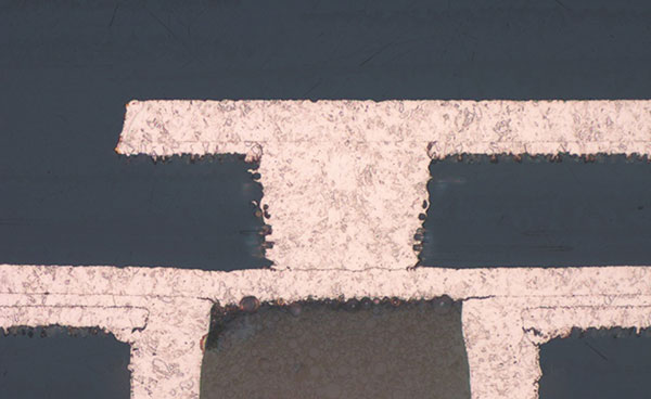
Figure 9. Passing stacked microvia structure.
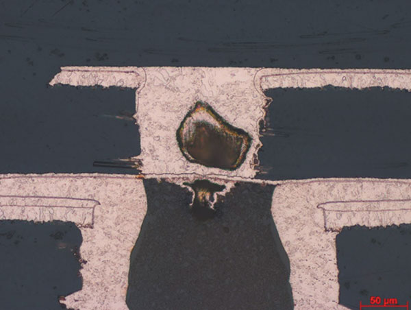
Figure 10. Poorly formed microvia.
FIGURE 11 is a microvia on top of a buried via with a 5-mil offset from fabricator A that we will take a closer look using focused ion beam (FIB) milling and a scanning electron microscope (SEM) for high magnification images. Both Figures 11 and 12 are from an optical microscope.
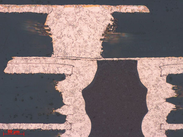
Figure 11. Cross-section of a failing microvia from Fabricator A.
FIGURE 12 shows dark boundaries above and below the cap plating layer. This indicates there may be separation, but it is very difficult to tell at these magnifications.
In FIGURE 13 the sample is rotated so the FIB cut can mill across the plating boundaries at the base of the microvia. After the milling is performed, SEM imagery can be used to get a very good look at the plating boundaries. In FIGURE 14 the separation occurring at the electroless copper layer between the target pad and the electrolytic copper is becoming more obvious.
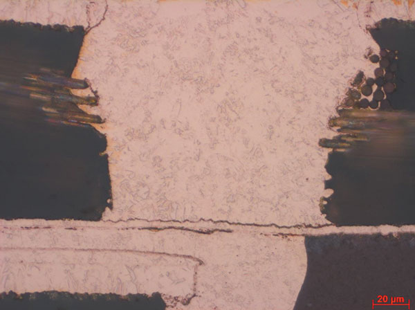
Figure 12. Higher magnification of the previous figure.
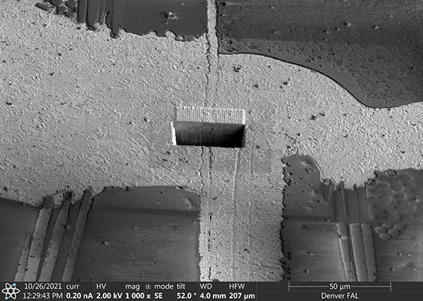
Figure 13. FIB cut across the plating boundaries, 1,000x.
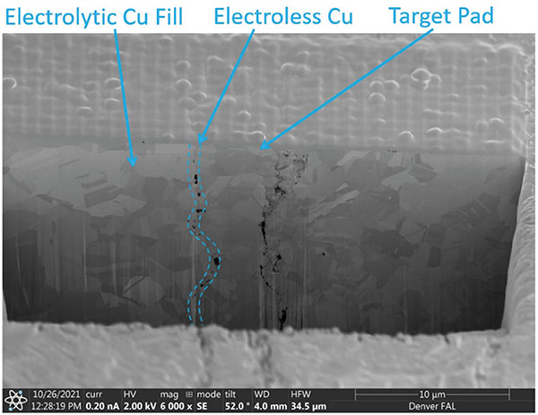
Figure 14. Previous figure at 6,000x.
FIGURE 15 focuses on the voiding occurring in the electroless copper layer. The copper grain structures do not bridge the plating boundaries. This is not a good sign the copper formed properly. Ideally, these crystal structures form across the boundary, but due to the separation they were not able to.
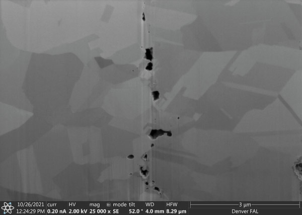
Figure 15. Voiding between the electrolytic copper fill and target pad, 25,000x.
The results from Fabricator B have not been discussed because almost all coupons passed testing. One coupon, however, failed thermal stress testing. This coupon was cross-sectioned, and the results (FIGURES 16 and 17) using an optical microscope look very similar to Figure 9 at lower magnification. This shows it may be difficult to determine pass/fail criteria for microvias using only cross-sectional analysis.
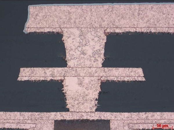
Figure 16. Cross-section of a stacked structure from a failing coupon of Fabricator B.
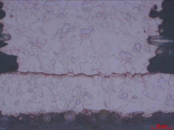
FIGURE 17. Base of the microvia from the previous figure at 1600x.
When looking at the optical microscope and SEM images of this microvia, the separation occurred between the thin electroless copper plating layer and the electrolytic copper fill, which can start to be seen in Figure 17 and becomes much more apparent in FIGURE 18. The separation can be seen in more detail after the FIB cut in FIGURES 19 and 20. There is suspicion that oxidation occurred between this boundary, but energy dispersive x-ray spectroscopy (EDS) was not able to verify this. One last item to point out is the thin layer of material in the separation: this is redeposited material from the FIB milling process and is not a part of the fabrication process.
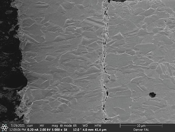
FIGURE 18. The previous figure rotated 90° CW at 5,000x.
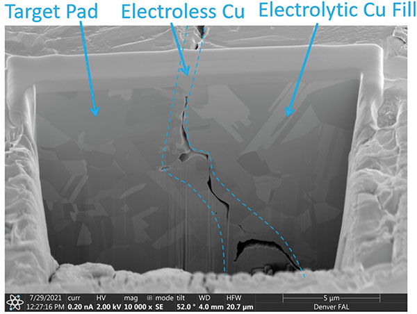
FIGURE 19. Plating boundaries after the FIB cut, 10,000x.
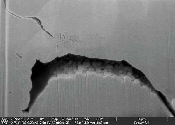
Figure 20. Separation in the plating, 60,000x.
In the future, transmission electron microscopy (TEM) may be used to help pinpoint the exact location of the electroless and confirm where the separation is occurring. In Figure 19 the separation occurs between the electroless copper and electrolytic copper fill, yet in Figure 14 it is not as clear.
Conclusions
Through extensive testing of hundreds of D-coupons representing various microvia diameters and pitches, some correlation came to light. Electrical continuity testing showed much better yield for larger diameter vias, yet it should not be relied on for screening microvia reliability because it does not expose the microvias to the environments they are most vulnerable to. Thermal stress testing yielded better results with larger diameter microvias and greater pitch microvias. These yields were greater than 90% for staggered microvias separated by at least 10 mils center-to-center, and the 6- and 7-mil diameter microvias with aspect ratios of approximately 0.75:1 and 0.64:1, respectively. The data show designing with an aspect ratio less than 0.75:1 combined with a diameter of 6 mils or greater and separation of 10 mils or more provides a more robust yield, even from a less-capable fabricator. The second fabricator with a more robust process yielded good results on almost all via constructions, including 5-mil stacked microvias. The next phase in this project will be to fabricate panels from more fabricators and run the same or similar testing to get a better idea on what the limits are within our domestic supply base. •
Acknowledgments
The authors would like to thank coworkers Curt Ricotta and Mitchell Hopper for their support and expertise. They were a huge help with failure analysis, including microsection and FIB work. We would also like to thank our fabricators for partnering on this effort and the team at CAT for its help in developing the test plan and performing thermal stress and thermal shock testing.
References
1. D-Coupon Generator, http://cat-test.info/d-coupon.
2. IPC-TM-650, method 2.6.27B, February 2020, www.ipc.org/test-methods.aspx.
3. IPC-6012E, Qualification and Performance Specification for Rigid Printed Boards, March 2020.
4. IPC-6012ES, Space and Military Avionics Applications Addendum to IPC-6012E, Qualification and Performance Specification for Rigid Printed Boards, April 2020.
5. IPC-TM-650, method 2.6.7.2C, March 2020, www.ipc.org/test-methods.aspx.
6. IPC-9252B, Requirements for Electrical Testing of Unpopulated Printed Boards, September 2016.
Ed: This work is adapted from “Microvia Reliability Testing Utilizing D-Coupons to Understand Best Design Practice,” which was first published in the proceedings of the 2022 IPC Apex Expo technical conference, and is published with permission of the authors.
Kevin Kusiak is associate fellow, PCB engineering, and Scott Bowles is electronics PMP materials engineer, senior staff at Lockheed Martin (lockheedmartin.com); This email address is being protected from spambots. You need JavaScript enabled to view it..
PCB West: The leading technical conference and exhibition for electronics engineers. Coming Oct. 4-7 to the Santa Clara (CA) Convention Center. pcbwest.com


