Effective strategies for calculating rogue wave noise levels.
For about 20 years, PDN design and analysis focused on the target impedance method. In recent years, additional considerations surfaced about rogue waves, but more as a general discussion. Here we present a new design/analysis method for estimating rogue wave amplitudes we can compare against the digital chip specs for design verification.
Electrical designs must be verified against possible worst-case conditions. For power distribution networks (PDN digital chip supply rail), this is typically done by comparing their impedance profiles against a target impedance requirement. From recent research and publications, we know the target impedance method for analyzing PDN design does not always predict the worst-case noise voltage because different frequency components of the chip supply current load steps can superposition on top of each other. This is sometimes called rogue waves (RW).
The industry has been evaluating different approaches to dealing with RWs: for example, adjusting the target impedance or flattening the impedance profile. Adjusting the target impedance is not sufficient because cases can occur when an adjusted target impedance is already met by the original design’s impedance profile, but it still fails with RW noise amplitude that’s too large. The whole impedance profile would need shifting down, not just the target impedance line. That is not easy to do. Achieving flat impedance profiles (Q < 0.5) on real digital designs is impractical. For a board designer, a more practical approach is useful to help with the initial component selection and checking the design at the early stage (when the schematic is being drawn) for a pre-layout pass/fail criteria, while not yet considering spatial or post-layout data.
In addition to the target impedance crossing criteria, additional criteria are needed for the designer, namely checking whether the worst-case noise amplitude (RW) is larger than the maximum allowed noise or not by using a crafted worst-case excitation waveform in simulation. We can perform this new type of check by computing the required excitation from the simulated PDN impedance profile. A known method for this is the reverse-pulse technique (RPT) that computes a wide band waveform consisting of rectangular load stepping with specific timing detail. This method requires the use of FFT/IFFT and accurate integral calculus to generate a step response, only correct if the PDN impedance profile was sampled in a linear fashion down to DC. That poses computational resource challenges and is impractical for everyday design projects.
This article introduces new methods. First is the case of implementing the RPT with a log-scale impedance profile that can be computed on 1,000 samples instead of millions of samples, but it is inaccurate. On 1,000 time domain samples (post-IFFT), we could not accurately display both a 100MHz and a 100Hz waveform. We investigate how inaccurate it is, or whether the inaccuracy might be acceptable in practical digital design cases.
The other new method is the multi-tone technique (MTT) that detects the frequencies of the impedance profile peaks and automatically places periodic excitations to each peak. This works on log or linear scale and does not require FFT or accurate integral calculus, but produces a theoretical signal. It is more like a system vulnerability check, rather than an actual test vector like the RPT.
Both the MTT and RPT seem to “attack” the PDN impedance profile at high-impedance areas, but with different strategies (FIGURE 1). MTT only focuses on peaks. RPT has a complicated distribution partly focusing on peaks, plateaus and other areas. On digital board VDD rails, we don't see multiple sinusoidal excitations. Instead, we have load current stepping/toggling between two levels. From recent publications, we know rogue waves can be created like this: The PDN can be excited with one toggle rate or frequency; it resonates. Then we suddenly change the toggle rate while the system is still resonating on the old frequency on stored energy (forced response), so the voltage response to the old and new frequency are super-positioned to create a larger wave: a rogue wave.
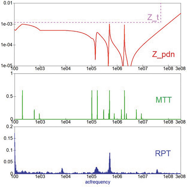
Figure 1. Spectrum comparison of MTT and RPT excitation waveforms, both computed from the same impedance profile.
Likely the main requirement of an RW is to present different frequencies at different times, sequentially, relying on recent remnants of resonance from stored energy. The target impedance method only ensures a single frequency component will not cause larger than the allowed voltage disturbance (percentage of VDD). To test and demonstrate different features, phenomena and corner cases, the PDN model had to be tuned differently with different capacitor and VRM parameters.1,2,3,4
Further, it will be demonstrated how these complex procedures can be automated with a single software tool: either Keysight ADS or the open-source QUCS. They serve as circuit simulators, SI-simulators and Matlab-like mathematical computational engines in one, allowing us to create custom equations and waveform processing. Normally we create templates, then reuse them in design projects.
The quality factor (Q) describes how under-damped an oscillator or resonator is. It is the ratio of the energy stored in the resonator to the energy lost in one radian of the cycle of oscillation. With higher Q peaks on the impedance profile, the oscillations die out more slowly. This means it oscillates longer, while the load switches the excitation to another resonant frequency that in turn increases the chances of creating a rogue wave. This is why often there is a focus on flattening the impedance profile to prevent the resonances from lasting too long. If we want energy loss to 0.1x in half period (3.14rad), then a Q < 1/(1-(0.1^(1/pi))) = 1.92 limit is required. For 0.2x energy remaining, we would need Q < 1/(1-(0.2^(1/pi))) = 2.5 limit. That is often achievable with 100nF or larger capacitors, but 0.2x remaining amplitude after half-period is not a guarantee to zero rogue waves. Our simulation template can check for Q factor between capacitor value pairs analytically. This does not compute the RW voltage amplitude; it provides a vague measure for RW probability.

The Reverse-Pulse Technique
A more common method for worst-case voltage response, or rogue wave computation, is the reverse-pulse technique (RPT). This requires FFT, IFFT, differential, integral and time (vector) reversal computations that would only be correct or accurate when using linear sampling on both the frequency and time domains. With logarithmic frequency sampling, we expect huge inaccuracy or distorted curves, but the spectrum of the excitation waveform aligns exactly with the peaks and high-impedance areas on the impedance profile, so maybe it is not that bad. A linear scale RPT down to DC would require at least 100,000 or, more likely, millions of frequency points to have decent resolution at a wide frequency range that is prohibitive in most simulation tools, especially the free ones. The way RPT is described requires an experienced engineer to assess waveforms, enter data manually, make decisions and use multiple tools.
This could also be automated using post-simulation equations in Keysight ADS or in the open source QUCS.
One attempt to compute a 100,000-point linear scale RPT on QUCS resulted in the simulation freezing at the vector reversal operation. Further simulations were conducted using a reduced bandwidth, reduced sample size, linear sampled RPT between 10kHz and 10MHz, plus a DC point on 1,000 points (10kHz even spacing) run in five minutes on a low-power laptop. Assuming a flat plateau created by VRMs, the DC value was the real value of the lowest frequency sample (10kHz).
The impedance profile as a numeric vector, or “waveform,” is processed through several steps to get the voltage response. From the AC circuit simulation result, the complete complex conjugate symmetrical spectrum with DC component had to be constructed at the size of 2^n or 2,048 samples for the FFT/IFFT to work correctly; that requires a 1,023-point AC simulation. The symmetrical spectrum as a vector was built as [real(Zpdn[0]),Zpdn,0,conj(Zpdn_rev)]. First we compute the step response:

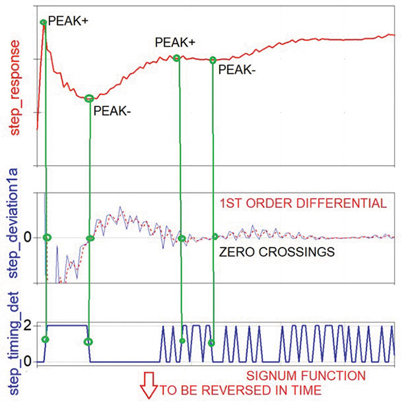
Figure 2. Timing extraction in RPT.
Then detect the voltage fluctuation timing on the step response; then create a toggling load step waveform; then reverse the timing of it (vector reversal). This is the excitation. In the QUCS template, the timing extraction (FIGURE 2) was done by computing the 1st order differential calculus of the step response, then chopping it up with a comparator (using the signum function). In other words, the positive and negative peaks are turned into zero crossings, then vertical edges of a square waveform. Then we can compute the response to that excitation:

Finally, we can measure the amplitude of this noise waveform by computing the maximum value minus the minimum value. All RPT equations can be seen in FIGURE 3.
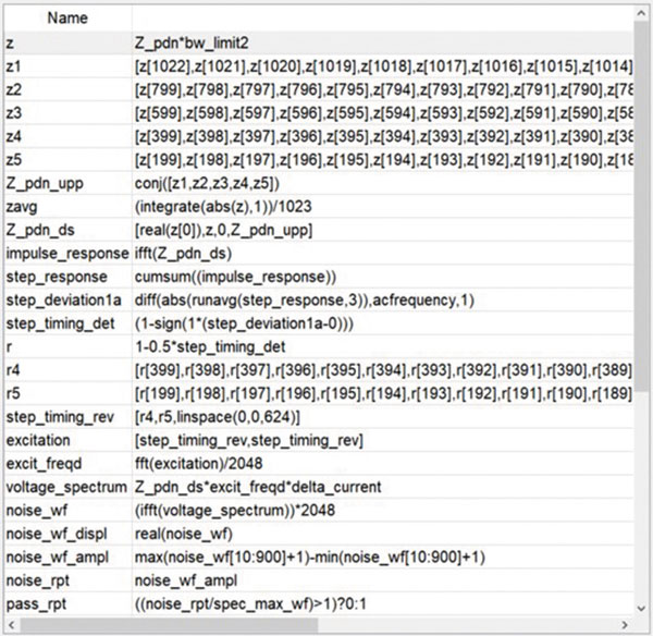
Figure 3. RPT equations.
Limitations. Sometimes the RPT picks up on the very high-frequency end, but that is not realistic; it’s overly pessimistic because every digital board PDN has very high impedance at very high frequency. In fact, they have infinite impedance at infinite frequency. The solution is to decide the frequency range of interest and bandwidth limit of the impedance profile before allowing it to be processed by either RPT, MTT or another technique. This also makes sense for simple target-impedance checking, as the impedance profile will cross the target impedance line at high enough frequency no matter what. The examples above were between 10kHz and 10MHz, so this issue didn’t occur, but on real design verification, we often go up to 50 to 500MHz with the analysis. Very few chip datasheets mention this bandwidth limit. If they do, it is typically 20 to 50MHz. My final QUCS template implements a bandwidth limiting function.
While testing different PDNs with LOG-RPT, especially the smoother ones, it was observed the time domain waveform seems to fly off near the last samples, causing the peak voltage measured to be higher than the main fluctuations seen throughout most of the waveform. This is likely a computational artifact. We can apply a window function on the waveform and only check the maximum and minimum peak values in the middle 90% of the samples.
In a test done with both QUCS AC-sim and LTspice transient simulation, the windowed version seemed closer to the Ltspice results. There was no VRM in this model, as LTspice does not support S-parameter files. In Ltspice we get a step response curve. By measuring the first two positive and first negative peaks, we can calculate the rogue wave amplitude as described in the original reverse pulse technique. Ltspice uses linear time sampling and no transformations, so it’s accuracy can be used as a reference, except it cannot handle measured VRM S-parameter models, so Ltspice is only useful here as a method reference with an RLC PDN model, not for real design validation.

The Multi-Tone Technique
The MTT avoids the accuracy (in logarithmic scale) or computation resource (in linear scale) issues within the reverse pulse technique (RPT) and provides a simple, fast way for a board design engineer to check the design for rogue waves with a pass/fail output. MTT sums up all the peaks (tones) multiplied by the load step automatically, then checks if the RW amplitude is larger (fail) or smaller (pass) than the max allowed noise from the datasheet. The MTT assumes these “tones” will be applied sequentially to the DUT, relying on stored energy, creating the rogue wave. Therefore, it is inappropriate to compute a time domain waveform from it using IFFT due to the inaccuracy of the logarithmic sampling and the lack of sequencing.
The noise voltage is:

While the maximum allowed peak voltage is given as a percentage of the VDD voltage:

Then the target impedance line is:

Instead of manually reading the frequency values of the peaks from an impedance curve, we can automate all that with waveform processing equations while remaining in the frequency domain. That is the point of the MTT. Since this method does not use FFT/IFFT or normal differential or integral calculations, accuracy should not be an issue. In regular differential and integral calculations, the resulting sample values are dependent on the gap width between the samples. Therefore, the gap must be accurately accounted for in appropriate units (Hz or ns), and each gap must be equal. None of the calculations below care about the gap widths. We only use differential computation to obtain frequency information for the creation of frequency domain Dirac Delta pulses, not to obtain accurate voltage levels. Accurate voltages are obtained through simple multiplication. We only do integral calculation to sum the levels of a few Dirac-like pulses, regardless of the frequency separation between them. It is more of an intentional misuse of integral calculus.
Step one: System model and simulation. Simulate the PDN model using the AC simulation feature. The system model in a schematic format in FIGURE 4 consists of a 1-amp AC current source excitation at the chip, capacitors provided as RLC parameters and S-parameter models for VRM (measured with VNA or manually created S-par file) and PCB power planes (from any 2-D field solver, a rectangle with estimated major X/Y dimensions). The VRM model would ideally be measured on a chip vendor’s evaluation board after we have carefully removed all smaller decoupling capacitors. We can post-process the S-parameter file in a partly automated Excel template created for this, with averaging or filtering – or replacing the upper frequency range with a 20dB/d slope. We could alternatively use a theoretical handwritten VRM S-parameter file. Several were provided with the template. The equation-controlled RF block converts the shunt through a 2-port S-parameter file of the VRM into a 1-port impedance part.
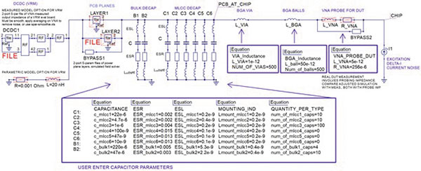
Figure 4. AC simulation model schematic, complete PDN.
The measured S-parameter models of VRM evaluation boards are usually very noisy, with hundreds of sharp peaks and valleys (grass) that confuse the MTT algorithm. To mitigate that, we must take the measurements with strong averaging or filtering to smooth the curve or post-process (smoothing) the measured model with an Excel file (created for this project and template) before inserting it into the PDN template. It also makes sense to completely replace (cut off) the higher frequency portion with a 20dB/decade inductive slope above a user-selectable threshold. Its desired effect can be seen in FIGURE 5. Both the smoothing and the cutoff are partially automated using an Excel template included with the QUCS template.
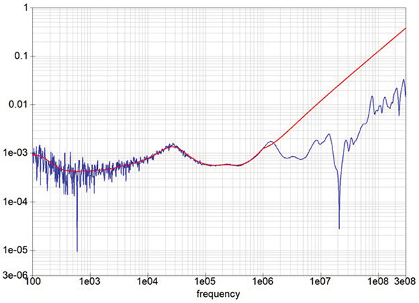
Figure 5. Post-processed version of a measured VRM model, with smoothing and high-frequency cutoff (at 1MHz).
Step two: Intermediate results. The simulation result is a Z_pdn(f) impedance profile stored inside the simulation tool as a vector with 1,023 elements as complex impedance values at distinct frequency points. An example can be seen in FIGURE 6 that uses a simple manually created theoretical VRM model, instead of using the measured VRM model. The capacitor values were tuned for demonstration purposes such that several peaks almost touch the Z_target line, not violating it, but they will violate maximum noise due to rogue waves, as we will see later.
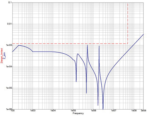
Figure 6. A complete PDN impedance profile with limited target impedance and manual VRM model.
Step three: Post-process the waveforms. In both ADS and QUCS, we place the equation component in the schematic that can contain multiple equations for computing and transforming post-simulation waveforms. We create waveforms from waveforms. After several steps, we can do a min./max. measurement to get the information we seek, like peak voltage. This is a creative process. FIGURE 7 shows the series of equations, while FIGURE 8 shows the intermediate waveforms graphically.
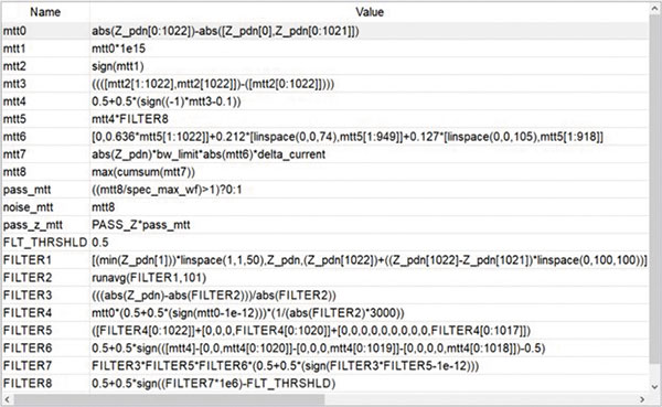
Figure 7. The equations for the MTT.
First we compute a discrete differential of the impedance profile by subtracting each sample from the previous sample. Then we magnify the results excessively to create vertical-looking edges (and zero-crossings) at the same frequencies where the impedance profile had peaks. Then we cut off the waveform at +1 and -1 levels using the signum function. After this we create a waveform that has little Dirac Delta 1 sample-wide pulses, where previously we had edges, using another discrete differential. Now we have negative Dirac pulses at the parallel resonances and positive ones at the series resonances, plus one pulse at the lowest frequency (to be removed).
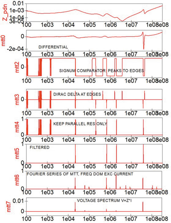
Figure 8. Intermediate waveforms from the equations.
After this we flip the curve upside down and eliminate the series resonances. This waveform is basically the excitation with multiple tones, but we need to apply two more steps: filter out the Dirac Delta pulses at the small impedance wrinkles and apply a Fourier series to make it more realistic. This is the load current spectrum of the excitation. Then we compute the voltage spectrum seen on the PDN as V = Z_pdn*excitation*Idelta*bw_limit.
Finally, we compute the sum of all voltage peaks using cumulative sum (integral), also known as the superposition of all resonant voltage response waves. We then compare the noise amplitude against the original datasheet specification and determine whether the design is a pass or a fail.
Even using a post-processed, smooth VRM S-parameter model, the impedance profile still has hundreds of micro-peaks (wrinkles) that throw off the MTT algorithm. To mitigate that, a FILTER algorithm was created that only allows big and sharp peaks. It computes the peak height at the detected frequencies (through relative impedance deviation, distance from a moving average); it computes its sharpness (steepness of the left side of the peaks through differential and a shift) and removes duplicate peaks. Then a carefully selected threshold is applied to ignore the smaller peaks. Finally, the filter is applied halfway in the MTT process, and only the more pronounced (tall/sharp) peaks make it into the final spectrum.
Digital board PDNs are not excited with sine waves. We only have digital chips generating load current steps or toggling, like a square wave or a pulse sequence. For a square wave, only about half the energy is applied at the toggling frequency, so the MTT tones should be reduced and replicated at 3x/5x/7x harmonic frequencies with 2/n*pi amplitudes, as a Fourier series. The main tone is 0.636 high; the 3f tone is 0.212 high with a 73-sample shift (when using 100Hz to 300MHz on 1,023 samples); the 5f tone is 0.127 high with another 30-sample shift, basically dispersing the energy in the spectrum to be more realistic.
Using a linear sample shift as frequency multiplication only works in log scale simulation, so a LIN-MTT with Fourier series would not be accurate. Both the original MTT – and even the target impedance method – wrongly assume the full energy of a single toggle rate excitation can appear 100% at a single frequency point. So, the MTT is adjusted with the Fourier series. Note the target impedance method also needs relaxing for the same reason, by raising Ztarget by 57%, even though we never do that for the sake of simplicity.
In one example (100Hz-300MHz, LOG 1,023 points), we got 26.7mV rogue wave amplitude with MTT and 16.1mV with RPT. This impedance profile in Figure 6 should not result in anything higher than 12mV noise, since the whole curve is under the target impedance line that was computed assuming 12mV noise (VDD*tolerance%). But it does, due to rogue waves created by a multi-frequency excitation at the parallel resonant frequencies.
A Comparison
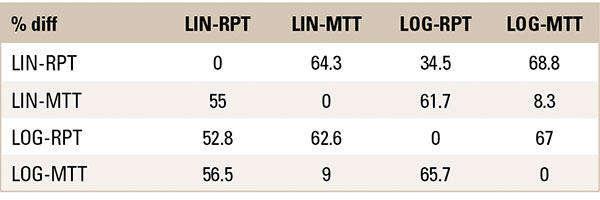
A final relative percentage deviation table between four methods (16 combinations) was simulated using parameter sweep at 18 component value combinations in a reduced range between 10kHz and 10MHz on 1,023 points. Both linear and logarithmic frequency sampling were used. The capacitor values were adjusted as 0.1x-1x-10x in a parametric sweep simulation. One capacitor remained constant, and two manually created theoretical VRM models were used: 0.25mΩ and 2.5mΩ plateau. It seems the different types resulted in very different noise levels, as seen in TABLE 1. The logarithmic RPT and MTT can differ as much as 67%, but, in most cases, around 20%. The LIN/LOG MTT differ a few percent only as a result of the interpolation of the VRM model.
Table 1. Maximum Difference Found Between Methods
Automated PDN Design Through Optimization
With pass/fail variables for the rogue wave amplitudes and target impedance, we could create a simulation that automatically adjusts capacitor quantities, instead of values – as it’s more practical from a selection of eight different catalog parts – to produce a design that meets all the requirements. This can be done using a simulation called optimization that reruns the AC simulation 100x with different pseudo-random component parameters (individual capacitor quantities), while looking to satisfy a set of user-entered goals.
Both the AC-sim and the OPT simulation controllers are placed in the QUCS (or ADS) model schematic. QUCS uses an optimizer simulator that is a separate open source project called ASCO. It had to be fixed to work with this PDN template. While the individual capacitor quantities are controlled by the optimizer, the VRM model had to be manually swapped out and rerun. Optimizer goals were the pass/fail variables for Ztarget and MTT to be > 0; total MLCC cap quantity equal to the number of power pins on the ASIC; bulk cap quantity less than a user-defined maximum; and a flatness metric limit to help with other goals indirectly.
We can measure the flatness using several arbitrary metrics computed from the impedance profile, then combine them into a single number (FIGURE 9). (Another paper called them “scores.”) We can compute a fitted impedance curve as a moving average to cut between the peaks, then compute the deviation from it in relative terms. Then we can compute several further variables from that and from the impedance phase curve. Phase differential is intuitively related to the quality factor. The area under the relative impedance deviation is computed with definite integral calculus. The peak heights and peak sharpness for parallel (positive) and series (negative) resonances can also be obtained as Dirac-like pulses and summed up automatically with cumulative sum. The template computes all these with a series of intermediate waveforms using differential, integral, signum and other functions. (The only reference I found to flatness requirement is the Q < 0.5 from literature, or the calculation above for Q < 2.5.) Instead of using Q or flatness for pass/fail check, we can more easily use a combined flatness metric as an additional optimizer goal that may or may not help the optimization process with the main RW amplitude pass/fail goal indirectly. Multiply the different scores, apply 1/x, logarithm and multiply by 20 to create a single flatness metric ranging between 1 and 20.3,5
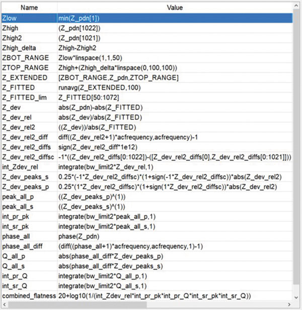
Figure 9. Flatness metrics computation.
In one example, the MTT noise voltage amplitude was reduced from 64.9mV to 18.6mV, while improving the flatness score from 9.5 to 12.1, as the optimizer changed the capacitor BOM quantities from [10, 10, 100, 10, 10, 10, 4, 10] to [383, 75, 1, 9, 30, 3, 0, 15]. We can see in FIGURE 10 how the impedance profile became somewhat smoother, simpler and a bigger “V.” Practically, we can run the optimizer with MTT (30 min.). Then, if we are curious, we can run the AC-sim on the optimizer result BOM with RPT, but without the optimizer activated. The RPT with optimizer takes a day to run.
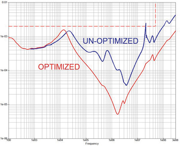
Figure 10. Optimized impedance profile.
Conclusions
All these methods create excitation waveforms with load current toggling between min./max. levels at different specific timing that create an excitation spectrum with a few automatically chosen peaks. All of these methods have blind spots. If the PDN is flatter and has no parallel resonances, then the MTT underestimates the worst-case noise compared to RPT that finds attack points on a flat impedance profile. On the other hand, if two parallel peaks are near each other, then sometimes the RPT misses one of them.
Probably the best strategy for a designer is to calculate the RW noise level with two to three different methods, all with logarithmic sampling for fast computation. Then take the worst-case result to be compared against the chip specs for final pass/fail condition.
Benchmark. On a low-power laptop, it takes a few seconds to run an AC simulation, a few more to run the MTT, 10 minutes to run the RPT and 100x the single simulation to run the optimizer. The optimizer with MTT can complete in one hour, with RPT 48 hours. The slowness of the RPT is caused by the QUCS tool’s deficiencies reversing vectors that are part of the RPT algorithm. Two vector reversals are required: one for the excitation waveform time reversal and one for creating a symmetrical spectrum before applying the IFFT. If they fix the known matrix multiplication bug, then we can multiply the vector with a rotated identity matrix, instead of bit by bit reordering, to speed up the vector reversal significantly. This allows us to include the RPT in the optimization goals.
A QUCS template was created for pre-layout design creation and experimentation by performing an automated check on target impedance and rogue wave amplitude. It can be used to help select the right decoupling capacitor values or quantities, voltage regulator part, loop compensation values (measure a retuned VRM evaluation board with a VNA and use the new S-parameter model) to meet the datasheet requirements from the ASIC chip vendor. The template is provided free to observe the details of the equations or to use it in product design. With QUCS and ADS, we can implement and automate the latest published scientific analysis techniques in our simulations. We don’t need to wait for tool vendors to implement them as hard features. For example, the inclusion of measured VRM S-parameter models or the computation of rogue wave estimation are not yet available in any commercial software as built-in functions. The MTT and LOG-RPT methods were demonstrated in pre-layout simulation. Since none of the commercial tools support them, neither do they support measured VRM models, and QUCS does not support post-layout extraction. A post-layout RW analysis considering spatial information could be conducted by extracting the PDN impedance profile from an SI/PI tool into an S-parameter file, inserting it into the QUCS template, disabling all planes and capacitors, running the simulation as usual.
References
1. Larry Smith, “Frequency Domain Target Impedance Method for Bypass Capacitor Selection for Power Distribution Systems,” DesignCon 2006.
2. Jae Young Choi, Ethan Koether and Istvan Novak, “Electrical and Thermal Consequences of Non-Flat Impedance Profiles,” DesignCon 2016.
3. Steven M. Sandler, Power Integrity Using ADS, 2020.
4. Steven M. Sandler, Eric Bogatin and Larry Smith, “Power Distribution Network (PDN) Impedance and Target Impedance,” EDICON 2018.
5. Jordan R. Keuseman, et al, “Capacitor Optimization in Power Distribution Networks Using Numerical Computation Techniques,” DesignCon 2021.
Tool Links
PDN template: https://buenos.extra.hu/download/PowerIntegrityDesign2_prj.zip
QUCS tool: http://qucs.sourceforge.net/
ASCO optimizer: http://asco.sourceforge.net/index.html
Istvan Nagy is senior specialist, electrical engineering at L3Harris Technologies; This email address is being protected from spambots. You need JavaScript enabled to view it..