Knowing the tradeoffs between electrical and materials constraints.
After components are placed and test strategy defined, if you find yourself worried there isn’t enough room left over to route traces and create power paths, there is no need to panic. This is a common condition caused by today’s dense packaging. The design requirements have transitioned into a need for multilayer PCB design technology. It is time for vertical thinking, where important z-axis strategy for routing and power planes is considered.
The term “topology” in the context of a PCB layer refers to geometric properties – copper shapes, clear areas – left over for routing or flooding with more copper. After placement of components, which may have taken up one or both external sides of the layout, a designer can more clearly see the remaining space for routing. With some experience and a keen eye to see enough remaining room between part footprints, a designer will begin considering whether the connections can be reasonably routed on the two outer layers. Often, advanced designers will set up and utilize the software’s autorouting capability to run a feasibility check for routing density. If it appears there is enough space to complete the routing, the design will most likely become a two-layer PCB.
If the component footprints occupy most of the area defined by the outline, however, the layout is most likely too dense to complete the routing on the outer layers. At this point, a multilayer design configuration must be considered to provide additional layers of copper to complete the routing.
From two to more. The term “stack-up” refers to the composition and layering order of the materials used in lamination of the PCB. The PCB stack-up is usually documented on the fabrication drawing as a diagram that provides the manufacturer with a quick view of the construction of the PCB. It can then be easily compared to the print, etch and electrical performance requirements of the PCB.
Selecting a sound PCB stack-up strategy is important because the etched and plated layers’ positioning and lamination from top-to-bottom affect not only the PCB’s electrical performance, but its mechanical performance.
Clock speed, edge rates, rise and fall times, and prevention of unwanted electromagnetic interference (EMI) are all considerations a PCB design engineer will have to address at some point. These issues are best identified early in the schematic stage. Once these constraints are identified, a designer may use a basic field solver or off-the-shelf impedance calculator to determine trace widths and spacing to meet the design for impedance requirements. At the start of the layout, the designer should do a feasibility check with the supplier to select trace widths for impedance-controlled lines; be sure to validate the values in the stack-up. Use care when adding information to the stack-up detail regarding three of the four variables mentioned above. Finished copper thickness is an important consideration regarding the various conductors’ current-carrying capacity. However, it is recommended the values of trace width, distance from reference plane, dielectric constant of the material (εr), and material sources be adjustable by the supplier. (Note: Using the stack-up detail to “document” the recipe for a working PCB prototype could create a procurement challenge. This is because materials used by domestic Western prototype shops are often not readily available offshore.)
When considering a stack-up configuration, be aware of the cost associated with the manipulation of the stack-up parameters to make the best decisions regarding routing density and power distribution. A project manager, along with the team of stakeholders, has already set many of the design and manufacturing goals for the PCB, which by the time the project has moved to the layout phase are called “constraints.” As the PCB moves to layout, two classic, diametrically opposed constraints need to be sorted out by the designer: design constraints vs. cost constraints. Design constraints define the performance of the electrical attributes of the PCB and usually are associated with increasing quality of materials and layer count. However, cost constraints define the profitability of the PCB. From the project stakeholder’s overall viewpoint, without intelligent adjustment and compromise to effectively meet both constraints, there is no product.
PCB Stack-up Cost-Adders
Copper thickness. The story of how copper foil thickness came to be referred to in ounces is an interesting one. In short, the reference to copper thickness was derived by how much one square foot weighed when being sold to the tinkers and workers in the roofing industry. For a PCB design engineer, the weight of copper is of far less concern than the actual thickness. However, with many in the electronics industry still referencing copper thickness in terms of weight, it is good to know how to convert. Memorizing the thickness of one-ounce copper can help.
1oz. copper thickness = 0.0014" – 35.56µm
A sweet spot for copper pricing and availability is half-ounce (1oz. divided by 2 = 0.0007 = 17.78µm). Thinner-base copper permits finer-pitch traces and more routes per layer. Thicker permits higher current-carrying capacity at reduced trace widths. In general, it is easy to understand copper is sold by weight, and therefore half-ounce copper should cost approximately half as much as one-ounce copper. This is mostly true, but the issue to be aware of here is availability. The two most commonly stocked copper thicknesses in production shops are half-ounce and one-ounce. Deriving a cost factor for four-ounce copper by simply multiplying by four is missing an availability factor: production suppliers may have to special-order copper outside the standard thickness ranges. This could add lead time to a project and cost much more than the copper itself in missed time-to-market and lost sales.
Adding layers. Beginning with a single-layer design as a basis, most are surprised to find a single-layer and two-layer PCB cost approximately the same for materials and processing. This is because the cost-adder of lamination does not need to be included.
If it is determined the outer PCB surfaces will run out of space for routing, a decision to switch to a multilayer design stack-up must be made. As a rule, layer pairs (two additional sheets of copper foil) are added. Perhaps one layer serves as a ground plane and another layer serves as a power plane. The average cost of adding a layer pair to create a four-layer PCB from a two-layer PCB is commonly estimated at double the price or a 100% cost adder. Therefore a $2 two-layer PCB will cost an estimated $4 if the design stack-up changes to four layers. The estimated cost of adding another layer pair to the design, increasing the layer count to six-layer, will increase the cost by another 50%.
This rule of thumb can work as an estimation tool for adding additional layer pairs to a point, but when increased accuracy in targeting cost estimates for higher count multilayer designs is required, it is best to obtain a quote from the PCB supplier that will be doing the work.
Shrinking traces. To keep stack-up layer count low, shrinking etched copper geometry is an option. Shrinking lines beyond the supplier’s sweet spot can lead to cost-adders, however. To keep cost-adders low, leave as much space as possible between densely routed traces for the supplier’s print-and-etch processing. When the trace widths and spacing fall below the supplier’s sweet spot, say 0.005" width with 0.006" spacing, the supplier may have to impose a 10% or more cost-adder to permit extra material required to cover any scrapped PCBs. Again, if increased accuracy of cost estimates is required, contact the supplier.
Epoxy-glass material types. One of the most common laminate material types used in the PCB industry is woven epoxy-glass, often referred to by its NEMA grade designation, “FR-4.” This material is supplied in many variable compositions and is available in many thicknesses, with the most common supplied at 0.062" (1.57mm) thick. IPC-4101, Specification for Base Materials for Rigid and Multilayer Printed Boards, is a good starting place for becoming familiar with FR-4 laminates. Many variables can add cost, but the most common adder is for material with higher processing temperature ratings above 130°C.
A temperature rating of 130°C attributed to the least expensive material may work well for a single-sided PCB design, which will experience limited heat cycles or “thermal excursions” during processing. However, a multilayer PCB with surface mount and through-hole components on both sides will be subjected to multiple thermal excursions during processing. To keep the material from exceeding the material’s glass transition temperature (Tg), causing possible through-hole barrel cracking and delamination, special additives are used to increase the material’s resistance to the effects of heat. Cost and availability for PCB laminates fluctuate greatly throughout the year. As always, if increased accuracy of cost estimates is required, contact the supplier.
As mentioned, selecting a sound stack-up strategy is important because the choices made by the designer can affect not only the PCB’s electrical performance but also its mechanical performance. In addition, knowing certain cost-adders related to the stack-up will help the designer make critical decisions while considering appropriate cost vs. performance compromises for the layout. Part two of this article will discuss DFM stack-up considerations; look for that in the next issue.
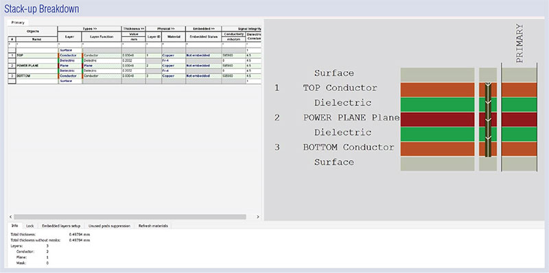
Figure 1. Sample stack-up configuration.
This excerpt of The Hitchhiker's Guide to PCB Design was written by EMA Design Automation. Download to learn more about PCB design stakeholders and real-world, actionable PCB design tips from industry experts (go.ema-eda.com/pcbguide).


