
What are void calculation tools telling you?
Although most will justify the cost of acquiring x-ray inspection capability for their facility based on the need for checking the reflow under BGAs, I suggest that, in terms of justification, looking for issues under QFNs could arguably be as important, if not more so. Use of quad flat no-lead (QFN) packages has become ubiquitous, and hidden QFN joints cannot be seen optically, post-reflow. Such joints may be more important to consider investigating as a matter of course because of the shape and design of the package and connections.
QFNs are planar objects and often contain a large central termination in the center (as a ground and/or for heat removal) with smaller I/O connections around the edges (FIGURE 1). In such a configuration, a relatively large volume of solder in the center will outgas during reflow. With the package flat to the board, and limited available pathways for the gas to exit, this may impinge upon how successfully gas is removed. Anecdotally at least, this would seem to be why there usually appears to be some level of voiding in the central terminations of most QFNs I have seen.
Voiding will also affect the distribution of solder in the central termination. For example, rather than the solder evenly spreading across the pad, voids will “concentrate” the same solder volume into the areas not covered by the voiding, potentially altering the offset height of the QFN from the board. In turn, this may tilt the package and lift one edge more than the other, affecting the quality and efficacy of the edge terminations. After all, the solder has to go somewhere! However, these potential height effects may not be of great concern, owing to having typically excess solder on the edge terminations that can potentially take up the slack of any package movement during reflow.
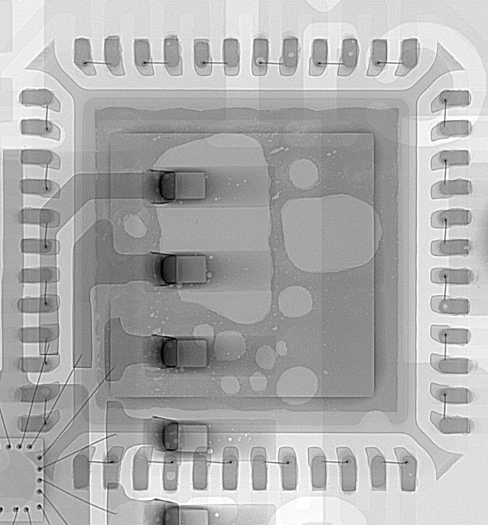
Figure 1. Top-down x-ray view of QFN. A second side component is also seen.
But even if there is (a lot of) voiding, particularly under the central QFN terminations, is this meaningful to the success or failure of the circuit, assuming all other (edge) joints are well made? Obviously, the true answer will depend on the needs for each type of board on its own merits, but if achieving zero voiding under a central termination may be very difficult to achieve in practice, what is an acceptable level of voiding for QFNs? With BGAs there are some suggested published guidelines, but there appears to be much less consensus for QFNs. What does the customer want or need? What does the device manufacturer suggest? My observation is often the answers to these questions are not clear-cut, or perhaps may not have been asked. For example, the manufacturer may say that up to XX% (and this may be as high as 50% voiding) is acceptable. From the customer’s side, if they have a specification they wish their board manufacturer to meet, this may be in line with the manufacturer’s recommendations, or they might demand a tighter tolerance. However, they may include additional caveats that the single largest void seen under the pad may not exceed a certain percentage, and also the largest void may not be located in a specific area(s). These latter criteria are often driven by the need to consider that a very large void in a specific location may impact the effectiveness of heat dissipation from the device and its position relative to other “sensitive” components on the board, rather than its electrical conductivity. When voiding is present, a gap between the package and pad could impact the effectiveness of heat transfer. In other words, might the presence of “excessive” voiding cause the component to overheat during use and/or cause a localized hot spot where it would not be desirable?
I suggest, therefore, that QFNs, and particularly their central terminations, need to be monitored and, if necessary measured, for the level of voiding they exhibit. Monitoring can be simply achieved in many x-ray systems by looking from the top down (Figure 1). By referencing the resulting image to an operator’s trained experience of seeing a range of good and bad similar examples, a value judgment can be made as to this particular sample’s acceptability.
Nevertheless, some numbers may also be required to satisfy a customer, as well as validate images used for operator training. To this end, many x-ray systems have the functionality to calculate the total void area for each pad (in percentage terms) as a function of the total pad area. This is achieved through a manual definition (by drag-and-drop) of where the pad is located. In addition, the software can identify and measure the area of the largest void. However, these calculations work best when no overlapping features are obscuring the QFN, such as if it were on a single-sided board. The reality, as seen in Figure 1, is you are usually not so lucky! In these situations, the void calculation software may allow you to also manually define and exclude areas from the pad area (FIGURE 2). This will reduce the total pad area size but ensure any voiding and density variations in those areas are not included in the voiding calculations. In Figure 2, the pad areas from the second side component have been removed. This results in a calculation of the total void area of ~38%, with the largest void at ~12%. As can be clearly seen, however, this approach has also excluded some “real” voiding that you would like to include. This is where using the partial CT (PCT) technique, if available on the x-ray system, allows a voiding calculation only at the device level without confusion from, or needing exclusions from, other features (FIGURE 3). (See my June 2018 column.) Using the PCT approach for our example (Figure 3) calculates the total voiding to be ~38% and the largest void as ~22%. Although the total voiding is the same as Figure 2, this is likely an artefact of this specific example and so should not be assumed to be the same. However, the single largest void has now almost doubled and may now exceed agreed-upon manufacturing specifications.
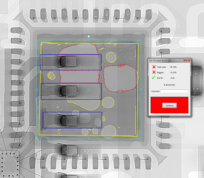
Figure 2. Void calculation of QFN central termination from a 2-D x-ray image. Three areas (in blue) have been defined and excluded from the pad area (in yellow) for calculation, as they have been deemed to relate to the second side component.
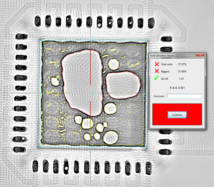
Figure 3. Void calculation of QFN central termination from a PCT model slice taken at the base of the QFN.
Some voiding under QFNs may be inevitable. Can you and your customer live with it? Is a process in place to review the voiding level and, as important, continue to maintain regular checks, as the process will naturally vary over time? Overall, is the voiding under the central terminations of a QFN at a level and position that is of concern? Check.
Au.: Images courtesy Peter Koch, Yxlon International.
David Bernard, Ph.D., is an expert in use and analysis of 2D and 3D (CT) x-ray inspection techniques for electronics; This email address is being protected from spambots. You need JavaScript enabled to view it..


