
When designing a rigid-flex, start with flex in the middle of a stack-up and move outward.
You’re designing a new rigid-flex. Devices are getting fanned out, via structures defined, and layer count is becoming clearer. You have determined how many flex layers you need from rigid section to rigid section. There are competing considerations on how those flex layers are configured: foil and dielectric thickness, bonded or unbonded, and where they will be in the stack-up of layers. All this impacts flexibility and how the part will bend in the installed application.
For today, let’s concentrate on where the flex layers land in the stack-up and the effect that can have on manufacturing and end-application use. Several strategies have rational logic and can be successful in select situations.
The most common and lowest impact is to place the flex at the middle of the stack-up. There are several advantages. First, it permits symmetry of the stack-up. Symmetry provides the opportunity for the flattest stack-up with the least tendency for bow and twist. This is more and more critical as component pitches get denser, and the size of BGAs and FPGAs gets larger. This is also the easiest to fabricate with the lowest cycle time, resulting in the lowest cost. If you can put the flex in the middle of the stack-up, this is the best option.
In some cases, the flex needs to be a little offset from top to bottom. For example, maybe you only want one or two rigid layers before you get to the flex, but then on the bottom you need four layers for the remainder of the design. Maybe you needed to do this to get some sensitive signals down the flex with the minimum amount of via distance and stub length. This is usually fine. There may be some increased tendency for warp, but it should be manageable.
In other cases, flex layers are moved close to the top or bottom of the stack because they may move the bend radius inward or outward. While this is true, it may only change the bend radius by 0.010" to 0.050". Hopefully the safety factor of the design is not so slim that this is the only option to achieve an acceptable solution. Depending on the total thickness on one side versus the other, this can result in warpage. Differential contraction of the materials during cooling after lamination causes this warpage. In many cases, this will impact assembly such that the surface of the panel is sufficiently warped, and solder joints are compromised. Without some post-processing (re-lamination), the part may not meet bow-and-twist requirements. Or if it does, it may warp during SMT assembly. I have seen cases in which the warpage was so severe we could not finish processing the circuit panel fabrication. We could not lay it down on a drill or send it through wet process equipment.
Another design strategy is to place the flex at the outer layer(s), like in FIGURE 1. While this can be done, it requires some technical consideration. For starters, using this example, there will be distortion of the flex material at the rigid to flex transition. Since there is no prepreg between layers four and five, the flex substrate for layers five and six will follow the topography above it. If layer six has traces that span from the rigid-to-rigid section, the conductors will distort as well. In some cases, when the traces are narrow, they may be prone to etch flaws, lowering yield. Resist coating, imaging and etch are affected by this distortion. Conductor distortion may also lead to assembly failures, if those conductors are bent tightly or are under strain. They may be more prone to cracking.
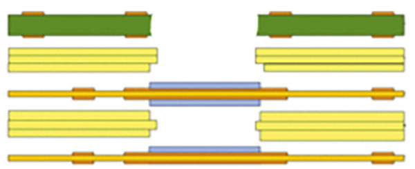
Figure 1. A design strategy placing flex at the outer layer(s).
Additionally, these types of designs cannot have through-vias that are filed and capped. This is because the planarization operation will almost certainly damage layer six and the associated substrate.
On the flip side, this type of construction does have an advantage from a conductive anodic filament (CAF) point of view. If the design has sub-0.8mm-pitch packages, and microvias are used from layer six to five, there is no risk of CAF between these vias, as the polyimide flex substrate has no weave; thus, it is not susceptible to CAF.
A variation on this theme involves the outermost layer as part of a flex core, but it only has copper features in the rigid regions of the board. Using Figure 1, layer five still has conductors in the flex and rigid regions, but layer six only has features in the rigid regions. Layer five gets etched at the substrate level, and since there are no conductors crossing the transition on the outer layer, the imaging and etching challenges for layer six are eliminated. This can work well and has been successful in very demanding applications.
The final consideration here for flex as an outer layer is whether or not the conductor pattern will get copper-plated during the hole-plating operation. If plated, flexibility will be impacted. If the layer is selectively (button) plated, then the outer layer will not carry as much current. This is not right or wrong, but something that needs to be considered.
Another option is to spread the flex layers apart, with rigid layers in the middle and flex toward the top and bottom. This is often symmetrical. Sometimes it is done to incorporate certain via structures. Other times it is done to try to create some physical separation between the flexes. Some say this separation eliminates binding of the flex when bent. I’m not sure I buy that argument.
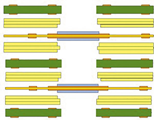
Figure 2. A design option spreading the flex layers apart, with rigid layers in the middle and flex toward the top and bottom.
This can be – and is – fabricated regularly but can increase cost somewhat. The manufacturer has to decide when to remove the internal rigid layers from the part during fabrication. In some cases, they may be removed at the innerlayer process, or near the end of the process. Both have pros and cons, but in either case, it impacts cost. This is because the manufacturer has additional operations to remove these materials from the middle of the stack that they do not need to worry about if the flex is at the middle. It can also impact layer registration if there are large openings routed into the internal layers.
When developing a stack-up, start with the flex at the middle, and work your way out, if you can. This provides the lowest cost, shortest cycle time, and most planar construction. When you need to deviate from the center, keep in mind how it might impact board fabrication and subsequent assembly.
Nick Koop is director of flex technology at TTM Technologies (ttm.com), vice chairman of the IPC Flexible Circuits Committee and co-chair of the IPC-6013 Qualification and Performance Specification for Flexible Printed Boards Subcommittee; This email address is being protected from spambots. You need JavaScript enabled to view it.. Co-“Flexpert” Mark Finstad is senior application engineer at Flexible Circuit Technologies (flexiblecircuit.com); This email address is being protected from spambots. You need JavaScript enabled to view it.. They welcome your suggestions.


