 Can switching the top and signal layers cause irreparable problems?
I have a two-layer flexible circuit that has worked well in my application for over a year. The top layer has signal lines, and the bottom layer is a plane. The flex is bent a few hundred times during its service life. Due to a recent change to other components in the device, I flipped the flex layers, so the plane is on the top layer and signals on the bottom. Everything else stayed the same. Now we are seeing cracks in the signal traces. Would just flipping the layers cause these conductor cracks when we never had issues before?
A lot of things could be going on here, so let’s examine the possibilities. First, it is important to understand what happens when a flex circuit is flexed. When a circuit is bent, there will be compression forces on the inside of the bend, and tension (stretching) forces on the outside. This is true on any material or laminate, whether it is a 1" thick plate of steel or a 0.005" flexible circuit. The thicker the material or laminate, the more extreme these forces.
Somewhere in the material core is a neutral bend axis, which is an imaginary zero thickness plane that does not see compression or tension forces (FIGURE 1). The material makeup of the overall structure will drive where the neutral bend axis will fall (and it is usually not dead center!). If the neutral bend axis is shifted toward the inside of the bend, the outer region of the material or laminate will be exposed to more extreme tension forces. The opposite is true if the neutral bend axis is shifted outward, in which case the inside of the bend would see more extreme compression forces.
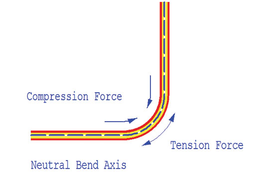
Figure 1. Every board has a neutral bend axis, which is an imaginary zero thickness plane that does not see compression or tension forces.
Many variables can impact where the neutral bend axis will fall inside a flexible circuit.
- Heavy copper layers or solid copper plane layers will resist tension and compression and will tend to shift the neutral bend axis toward those layers. A cross-hatched copper plane will have less effect than a solid copper plane.
- Thick polyimide layers (more than 0.003") will also resist bending forces and will have the same effect as heavy copper or plane layers.
- Multiple layers of any of the above materials will tend to cancel each other when placed on opposite sides of the neutral axis.
- As a rule, keeping the neutral axis close to the center of the stack will equalize tension and compression forces so that neither will become too extreme.
Refer to IPC-2223 for guidelines on bend ratios (bend radius to circuit thickness) to ensure the application conforms to industry-accepted criteria.
Let’s get back to the question. I am going to assume that in the original design, the signal traces were on the inside of the bend and now are on the outside. If that is indeed the case (which I suspect it is), those signal traces would have been in compression when the part was flexed, and the new design would put them in tension when flexed. I have found that small signal traces generally tolerate compression better than tension. This is even more true if the traces are very narrow (under 0.006") or very thin copper (0.5oz. or less). In addition, moving the plane layer to the inside of the bend will draw the neutral bend axis inward, causing more tension forces than the original design. I don’t know what the polyimide core thickness is, but if it is more than 0.001" or 0.002" that could be a contributor as well.
A few final items that could be causing the issues you are now seeing are copper type (rolled annealed vs. electrodeposited), copper plating (panel plating vs. pads only plating), and cover type (polyimide vs. flexible solder mask).
- Copper type. Rolled annealed (RA) will tolerate stretching and compression better than ED. I personally only use RA copper for any application that is more than just a one-time “flex to install” use.
- Copper plating. Pads-only plating will result in an overall thinner circuit by reducing copper thickness and cover adhesive thickness. Lower thickness equals lower compression/tension forces. Additionally, copper panel plating essentially negates the benefit of using RA copper, since the entire RA surface will be covered with ED copper. If the ED-plated copper cracks, it will propagate through the RA copper.
- Cover type. Polyimide covers will always outperform flexible solder mask in challenging bending applications.
My advice on this application would be to first look at ways to make the circuit thinner to reduce bending forces. This can be done by reducing polyimide core thickness, using thinner base copper, using pads-only plating instead of panel plating, etc. Next, make sure RA or HA (hyper annealed) copper is used, and ensure the grain direct of the copper is oriented parallel to the traces. Last, consider changing the plane layer from solid copper to a cross-hatched pattern, or eliminate the plane layer altogether and replace with a shielding film. In many cases, a shielding film can provide all the functionality of a copper plane and reduce the thickness associated with that plane by 50% to 75%.
Mark Finstad is senior application engineer at Flexible Circuit Technologies (flexiblecircuit.com); This email address is being protected from spambots. You need JavaScript enabled to view it.. He and co-“Flexpert” Nick Koop (This email address is being protected from spambots. You need JavaScript enabled to view it.) welcome your suggestions. The authors will speak on flex design and manufacture at PCB West in September (pcbwest.com).