 To avoid post-soldering delam, keep parts dry, and use plenty of adhesive.
I am experiencing flex circuit delamination. What is causing it?
Delamination occurs for a few different reasons. Very often, it happens during solder reflow during assembly. Usually this is due to moisture absorbed into the part prior to the soldering operation. Flexible materials absorb moisture, and during soldering that moisture can rapidly heat and expand, resulting in delamination. The first line of defense is prebaking prior to soldering. In a standard oven, just getting above the boiling point of water is good enough, so 225° to 250°F is plenty. Bake time can vary depending on circuit thickness, but two hours is a good start. Thick rigid-flex parts may need four to six hours. If parts are stacked in the oven, time may need to be added to ensure the parts in the middle of the stack dry out.
Once parts are dry, keep them dry. Flex materials will acclimate to the environment very quickly, so make sure to store dried parts in a dry environment. Limit the time parts are exposed to ambient conditions before soldering. Use of a desiccant chamber (dry box), or bagging and sealing, usually solves assembly delamination problems.
A different failure mode has occurred when using thicker film material where delamination occurs during soldering. In this case, the coverlayer is a thicker film, say 3 or 5 mils thick, over a thicker copper. Heat from the reflow operation causes the adhesive to soften, and residual stress in the polyimide film causes it to spring back to a flat state. It pulls the coverlayer away from the base laminate between traces, causing delamination. In these cases, the solution is to add adhesive or reduce film thickness.
Delamination is also experienced during hand soldering. It can be easy to inject excessive amounts of heat energy into a concentrated area as you move from pin to pin. To avoid this, try alternating soldering pins in different areas in the pin field. This can give one area some thermal relief, while soldering a pin in another area.
Laminate voiding. In some cases it is not actually delamination; it is non-lamination, or laminate voiding. Many times, this is design-driven. Often there is just not enough adhesive to do the job. This happens during a couple scenarios.
During lamination, void-free lamination occurs when adhesive flows off the top of the conductor and down in the “valleys” between traces, and the coverlay film conforms to the etch pattern to make up the difference. In most cases of non-lamination, the copper is too thick for the adhesive thickness selected. There is simply not enough adhesive to flow and fill the copper pattern. In these cases, the solution is to add adhesive.
Less often, the adhesive may have trouble flowing into tight spaces. For instance, what worked on 2 oz. copper with 0.020" spacing does not work when the spacing is only 0.007". When spacing gets tight, it is hard to exert enough pressure into the crevices to get the adhesive to fill them up. Again, adding adhesive can be the solution.
Another situation is when the coverlayer film is thicker, typically more than two mils thick. In this case, the film is stiffer and will not conform much. As a result, the adhesive has to do all the work. The best solution is to reduce the film thickness. If impedance is driving film thickness, it can be offset by adding adhesive. If there is a high voltage requirement, most applications are well supported by 2-mil film. The film is rated at or above 5000VDC/mil; few things need more than 10,000V of dielectric separation.
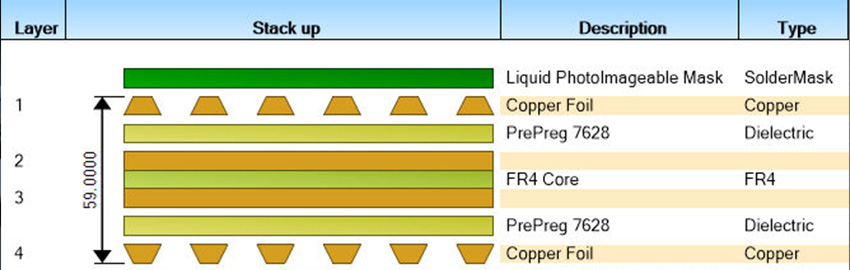
The examples above are all for coverlayer situations. Lamination voids are also common for bondply materials, which are films with adhesive on either side. These are used when bonding multiple flex layers together. In these cases, consider both copper layers, and how much volume needs to be filled in. The etched patterns on each layer have an impact; large planes do not consume much adhesive, but the small moats between the plane and isolated pads can be difficult to fill. It can also be a challenge to fill in two very dense signal layers facing each other.
The rule-of-thumb is to have at least 1 mil of adhesive for every ounce of copper. Usually that works, but keep in mind we are running a little thin when we do that. One ounce copper is approximately 0.0014", or 35µm thick, which is a bit thicker than the adhesive. To ensure void-free lamination, we recommend 2 mil adhesive for one ounce copper and an additional mil of adhesive for each additional ounce of copper.
Extra adhesive does add somewhat to overall thickness, but if there is a voiding issue, we can comfortably say some of the extra thickness will be consumed filling in the valleys. When extra adhesive is used, the coverlayer film tends to lie flatter. Also, extra adhesive will have minimal impact on flexibility, as the adhesive is very flexible. Swapping a mil of adhesive in place of a mil of film will actually improve flexibility.
To summarize, design the part with enough adhesive to flow and fill the crevices designed into the PCB. Once the boards are fabricated, keep them dry until it is time to solder the components. Following these two guidelines will dramatically reduce the potential for lamination troubles.
Nick Koop is director, flex technology at TTM Technologies (ttm.com), vice chairman of the IPC Flexible Circuits Committee and co-chair of the IPC-6013 Qualification and Performance Specification for Flexible Printed Boards Subcommittee; This email address is being protected from spambots. You need JavaScript enabled to view it.. He and co-“Flexpert” Mark Finstad (This email address is being protected from spambots. You need JavaScript enabled to view it.) welcome your suggestions. Listen to their recent podcast at PCBChat.com.