Microvias have a domino effect, increasing available copper and lowering resistance.
Today electronic devices typically use designs with complex requirements that only high-density interconnect (HDI) technology can meet. Component manufacturers support the move by making components with smaller pitches. Because they are using more I/O connections, larger FPGAs and ASICs operate at higher frequencies, and the sharper rise times require smaller PCB features. The HDI PCB process supports these requirements exceptionally.
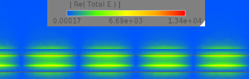
HDI PCB designs use microvias that offer a number of electrical benefits, and they also improve the power integrity of the assembly. This enhanced integrity comes from such sources and enhancements as decoupling capacitors, presenting a smaller mounted inductance, and chip pinouts requiring fewer perforations, thus delivering better performance from planes. The HDI PCB process also uses dielectrics of different thicknesses that reduce plane capacitance compared to conventional design.
Planning the HDI design. By permitting a combination of attributes targeted toward high density, the HDI process permits higher routing density per unit area in comparison to traditional PCB technology. In general, fabricators build HDI PCBs with a combination of one or more of sequential lamination, blind and buried microvias, and reduced trace width and spacing. Designers are most likely to apply HDI technology to products that must be compact and lightweight.
Microvias are a key aspect of HDI technology. Per IPC, microvias are holes with a maximum diameter of 150µm. Designers, in cooperation with fabricators, make multiple types of HDI stackups containing blind and buried microvias. This leads to the creation of high-quality HDI boards that are also low cost.
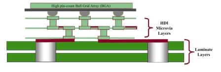
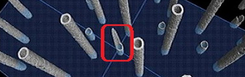
FIGURE 1. High-density, high pin count IC packages are driving the need for HDI designs.
HDI power integrity. When designing the power distribution network for an HDI PCB, the designer has a simple goal: minimizing the impedance between power and ground for the frequency range of the product. With the real estate available on the board for capacitors shrinking quickly and the presence of multiple voltage rails, however, this task can be formidable.
Designers must locate multiple capacitors, such as those between power and ground, between planes and traces carrying power and those for on-chip decoupling. Then one must consider the pins and vias needed to connect all these elements.
Very large electrolytic capacitors usually have minimum impedance at a frequency lower than that of smaller capacitors; beyond this frequency, the impedance increases. Since the parasitic inductance of the planes is very low, they behave as an effective capacitance, even at higher frequencies. Therefore, all these capacitances add up to provide the low impedance required between the power and ground for the operating frequency range.
For the HDI PCB design to be effective, the designer must minimize the loop area of the capacitor connection between power and ground. The best way to do this is to position the vias very close together, and also to place the capacitor very close to the power and ground planes. The HDI design process achieves this by enabling the designer to position connection vias within the capacitor pads.
Power distribution. Prolific use of microvias in the HDI design process makes a much larger routing area available to the designer. The major effect of this is a significant reduction of vias penetrating the innerlayers of the PCB. This also includes the absence of multiple anti-pads perforating the power planes.
The result is a larger area of copper available for the planes carrying both DC and AC current to the power pins. This results in a general lowering of resistance in the current path and lower areas where the concentration of current density is high. Moreover, this leads to each IC power pin facing lower inductance, so that switching currents reach them appropriately, while the decoupling capacitors perform adequately.
Use of blind microvias is a great advantage of the process, since this directly connects IC pins only to the necessary layers. This avoids placement of extra vias, and results in a huge overall reduction in the anti-pads. This also increases the amount of copper in planes carrying power.
Of course, it is not possible to avoid anti-pads totally in any PCB design, whether HDI technology or conventional. However, it should be noted the size of the anti-pads is greatly reduced compared to that of traditional through-hole vias. The reduction in size of anti-pads and overall reduction in their total number contributes to a significant increase in the amount of copper available on planes carrying power.
Implementing the HDI PCB design process offers several benefits, including improved electrical performance because of better routability, as well as reduced plane perforations. The substantial reduction in the number of vias and the presence of blind microvias in high-quality, well-designed HDI PCBs leads to significant improvements in power distribution within the board, improving its power integrity compared to the traditional board design. All this has the effect of making the board a low-cost HDI board overall.
Akber Roy is chief executive officer of Rush PCB Inc., a printed circuit design, fabrication and assembly company (rushpcb.com); This email address is being protected from spambots. You need JavaScript enabled to view it..
Register now for PCB WEST, the largest trade show for the printed circuit and electronics industry in the Silicon Valley! Coming Sept. 11-13 to the Santa Clara Convention Center.