After almost 150 years, Maxwell’s equations still have a strong influence on modern SI tools and methodologies.
In the late 1800s, James Clerk Maxwell formalized the wave theory of
electromagnetic radiation and arranged a set of formulae (called
Maxwell’s equations) to describe such wave motion
1.
Maxwell’s equations form the foundation of classical work in circuits
and electromagnetics. They portray the interrelationship between
electric fields, magnetic fields, electric charge and electric current.
Subsequently, these formulae illustrate the nature of interaction
between electromagnetic fields, conductors and dielectric materials.
The electromagnetic spectrum1 includes radio waves (< 3E9 Hz),
microwaves (3E9 to 3E11 Hz), terahertz waves (3E11 to 3E12 Hz),
infrared (3E11 to 4E14 Hz), optical/visible light (4E14 to 7.5E14
Hz), ultraviolet (7.5E14 to 3E16 Hz), X-rays (3E16 to 3E19 Hz) and
gamma rays (>3E19 Hz).

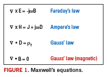
Maxwell’s formulae are available in several styles including time and
frequency domain versions
2. One form is presented in
Figure 1. In
Figure 1, E=Electric Field Intensity (V/m), H=Magnetic Field Intensity
(A/m), J=Current Density (A/m
2), D=Electric Flux Density (C/m
2),
ρv=Electric Charge Density (C/m
3), B=Magnetic Flux Density (W/m
2) and
ω=Angular Frequency (Radians/sec). Maxwell’s equations encompass a wide
range of applications and can describe electrical properties
2 of
interconnects.
Let us briefly consider the significance of one of these four great
laws of electricity and magnetism, namely Gauss’s law. It is formulated
in terms of continuous charge distributions and can be utilized to
derive Coulomb’s law
3. Gauss’s law is well suited for ascertaining the
electric fields at various points in space when the charges producing
the fields are symmetrically distributed. Such situations frequently
happen in the design of electronic components.
An example is offered by coaxial cable, which is widely used in
engineering laboratories and also possesses some interesting PCB
applications
4. For instance: (i) the pad for a PCB via and its
surrounding ground plane cut-out can form a very short section of a
coaxial line (allowing use of coaxial line formulae to achieve
impedance matching); (ii). Semi-rigid coax lines with very small outer
diameters are available that can provide a fully shielded path for the
signals on PCB in low-volume production, prototyping and reworks.
The coaxial cable forms a uniform two-conductor (controlled impedance)
transmission line and exact mathematical expressions exist for its
capacitance
2, impedance
4, and propagation delay in terms of its
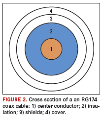
physical parameters. A coaxial cable includes four parts
5 as indicated
by
Figure 2.

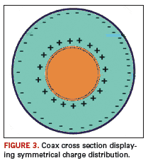
An enlarged view of an inner conductor and the surrounding
insulation/dielectric layer is illustrated by
Figure 3. Figure 3
demonstrates that the charges within the dielectric region possess
cylindrical symmetry. Gauss’s law can then be applied
3 to ascertain the
electric field inside or outside the cable. The field computation
results would then reveal how the cable affects the signal traveling
along its length, and how to ascertain the optimum cable parameters.

Sometimes the coaxial cables depart from an ideal symmetrical geometry
due to manufacturing6 limitations. Simulation may be then required for
determining various characteristics (such as propagation delay) of the
coax cable.
For complex geometries, Maxwell’s equations usually demand simulation.
Three types of electrical simulators
2 include: (i) behavioral
simulators, (ii) circuit simulators, and (iii) electromagnetic (EM)
simulators. The EM simulators are well suited for solving Maxwell’s
equations. Speed 2000 (Sigrity), Sonnet Lite (Sonnet Software Inc.) and
Maxwell (Ansoft) are among electromagnetic software programs.
A free version of Maxwell 2D software (called Maxwell SV) is available
from the Ansoft Web site. The program contains advanced 2D electric
fields, AC/DC magnetic fields and eddy-current solvers applicable for
analyses and the design of numerous electronic components.
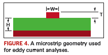
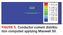
Let’s apply the eddy-current solver of Maxwell SV to compute the field
distribution inside a microstrip trace at a frequency of 400 MHz. The
geometry as depicted by
Figure 4 includes a trace having the following:
width W = 5 mils, thickness T = 2 mils, height H = 4 mils. The
substrate and conductor materials are FR-4 and copper, respectively.

The simulation outcome is presented by
Figure 5. Current density is
described by a color map (with red being the highest and blue being
lowest). The results indicate that current intensity is largest close
to the conductor surface, due to skin effect.

For skin effect analyses using Maxwell SV, one pitfall to avoid is not
to assign a “perfect conductor” as the material property for the trace
and the ground plane. A perfectly conducting structure (i.e., infinite
conductivity) allows only surface currents with skin depth approaching
zero. Subsequently, to produce accurate eddy current results, the trace
and ground plane need to be assigned finite conductivity (i.e., for
copper conductivity σ = 5.6E7 Siemens/m).
Skin depth (δ) is defined as the depth below the surface of the
conductor at which the current density decays to 1/e (approximately
0.37) of the current density at the surface.
It can be calculated2 via:
δ = 1 / sqrt (σπfμoμr)
[Equation 1]
Where, δ is in meter, σ is conductor’s conductivity (in Siemens/m), f
is frequency (in Hz), μo is free space permeability (1.257E-6 H/m) and
μr is conductor’s relative permeability.
For copper (with σ = 5.6E7 Siemens/m, μr = 1), a simpler equation can be obtained:
δ = 66/sqrt(f)
[Equation 2]
where δ is in microns and f in MHz.
At f = 400 MHz, for copper Equation 2 yields skin depth δ = 3.3 micron (or 0.129 mil).
The skin effect has important/practical applications in several
engineering branches such as design of radio frequency and microwave
circuits. The current distribution in most PCB interconnects will be
skin-depth limited
2, and resistance will be frequency-dependent for
frequency components exceeding 10 MHz. Skin effect can be measured
7 by
applying Time Domain Transmission (TDT) techniques.
The skin effect losses may be compensated8 by plating the outer
conductor surfaces with gold (for microwave/RF PCBs) to enhance
conductivity, or by increasing the width of traces (applicable for
logic PCBs) to enlarge the surface area.
PCD&F
Dr. Abe (Abbas) Riazi is a senior staff electronic design scientist
with ServerWorks (a Broadcom Company) in Santa Clara, CA;
This email address is being protected from spambots. You need JavaScript enabled to view it..
Acknowledgement
I would like to thank the members of Broadcom SI Council, especially Sam Karikalan (chairman) and Amit Agrawal (co-chairman).
References
1. Andrew Zimmerman Jones, “Electromagnetic Spectrum of Light,” About.com: Physics.
2. Eric Bogatin,
Signal Integrity – Simplified, Prentice Hall, 2004, pp. 23-26, pp. 109-192, pp. 340-342.
3. Peter Signell, “Gauss’s Law For Spherical Symmetry,” Physnet, MISN-0-132, Michigan State University.
4. “Introduction to Common Printed Circuit Transmission Lines,” Dallas Semiconductor/Maxim Application Note 2093, June 2003.
5. Howard Johnson and Martin Graham,
High-Speed Signal Propagation: Advanced Black Magic, Prentice Hall, 2003, pp. 513-514.
6. Timothy Hochberg and Henri Merkelo, “Propagation Characteristics of
Coaxial Cable with a Helically Wound Ground Shield,” 1996 IEEE, pp.
888-892.
7. Roy G. Leventhal and Lynne Green, S
emiconductor Modeling For
Simulating Signal, Power, and Electromagnetic Integrity, Springer,
2006, pp. 34 and 126.
8. Lee W. Ritchey, R
ight the First Time: A Practical Handbook on
High-Speed PCB and System Design, Vol. 1, Speeding Edge,
2003, p. 19.


