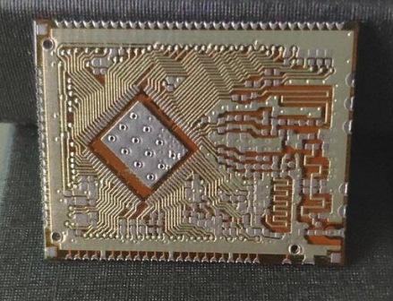
NESS ZIONA, ISRAEL – Nano Dimension today announced the world’s first side-mounting technology for additively manufactured printed circuit boards (PCBs).
The maker of additive printers said it can print and solder components to the top, bottom and sides of a PCB, resulting in as much as a 50% increase in board space when compared with conventionally manufactured PCBs.
The extra space afforded through side mounting permits more functionality on the circuit board. The company said this is particularly relevant for IoT and Industry 4.0 where customized designs and shapes are a growing demand.
“For applications like the IoT where innovation is paramount, creating new electronic products in shapes and sizes that were never before possible is liberating for design engineers,” said Amit Dror, CEO, Nano Dimension. “Because of this added real estate, more functionality can be generated from sides of the board that can also be used to connect with additional boards.”
Another important enablement of side mounting is the ability to create a specialized PCB that plugs into a socket mounted on a mother board. By printing this board and inserting it into the cavity of a second board, users can rapidly customize applications based on a generic motherboard.
Side mounting is ideal for applications such as modular antennas, creating non-standard packaging and innovative IoT applications. Future potential applications and benefits of Nano Dimension’s side-mounting technology include printing a horizontal ground layer on the z-axis, enabling the printer to produce higher performance antennas or multiple antennas with varying voltages within the board. This not only saves space but also creates limitless design possibilities.


