Conductive paste instead of microvias can lower drilling costs and scrap rates.
Printed circuit board design and construction is meeting integrated circuit packaging requirements through any-layer interconnection schemes using combinations of copper-plated-microvias and paste-filled interconnects in stacked and offset configurations. Used independently, both copper-plated and paste-filled interconnects have advantages for specific types of product structures, but when combined, the resulting design and manufacturing flexibility provide a path to bridge the divide between the IC and motherboard packaging requirements.
Applications for high-layer count, complex RF design, high-density-interconnect and rigid-flex combinations are already manufactured in high volume, but the continuous demand is for smaller, lighter, thinner and lower-power-consumption products. The industry is struggling with the complexity of mixed-mode, multiple-process-step manufacturing and cost-down targets. Paste-filled interconnects permit the joining of mode-specific cores (e.g., flex) or subassemblies in single or multiple laminations. This permits each mode-specific core or subassembly to be manufactured cost-effectively to best practices for that particular mode, and then joined into an integrated whole. This has the potential to significantly reduce time-to-market and manufacturing cost, and can enable assembly by breaking these complex structures into simpler mode-specific subunits that can be electrically interconnected at the end with paste-filled vias.
The demand for rigid-flex products is increasing. Due to the imbalance in the mechanical characteristics (such as coefficient of thermal expansion) of base materials with conventional methods, these products are complex and cumbersome. If a Z-interconnect scheme is employed, the rigid and flex subassemblies can be manufactured separately under their respective best-mode manufacturing techniques and then joined with a bonding layer containing paste-filled interconnects at high-Tg FR-4 temperatures (~180ºC). This same type of construction scheme can also enable the combination of multiple signal speed channels into a single construction. For another example, it would also permit the high-density portion of a circuit to be miniaturized, manufactured as an independent subassembly and then joined to the main portion of the circuit board so that the whole fits within the tight physical limits desired for a specific product.
High-density-interconnect with anywhere, any-layer interconnects is the core technology that enables the miniaturization required for the feature-packed smartphone market segment. As designs approach the need to have five or more outer buildup layers containing stacked copper-plated microvias, fabricators seek relief from the repetitive lamination steps to save time, energy and water resources and to maintain yield. By breaking the outerlayers into subassemblies and using paste-filled interconnect bonding layers to join them to the core construction, the number of lamination cycles can be reduced and yields substantially improved. This manufacturing strategy produces more products in less time within the same manufacturing space. Making HDI layers using state-of-the-art conventional practices and then joining them to the core with paste-filled interconnect bonding layers provides design freedom to the client, excellent electrical properties for the device and higher yields with a reduced number of lamination cycles to the fabricator.
Every layer interconnection (ELIC) and subassembly core-to-core interconnects are delivering:
- Tighter wring densities.
- Improved performance through shorter traces.
- Separation of low- and high-speed signal channels.
- Ability to join different materials in optimum press cycles.
- A framework for embedded components.
These assembly advantages, coupled with proper design, offer cost advantages when products are built in large-scale production or in low-volume, high-mix assembly lines. Here, the costs associated with manufacturing ELIC structures employing a Z-interconnect paste technology are outlined. Two example designs were chosen to analyze the cost of using this technology versus conventional interconnect. The first case is a small 10-layer board similar to most smartphone motherboards. The second case is a large 28-layer circuit board similar to those found in servers.
Activity-Based Cost Modeling
Activity-based cost modeling (ABC) and parametric cost modeling are the two dominant cost modeling methods. Parametric cost modeling is done by statistically analyzing a large number of actual results and creating a model that matches as closely as possible. This “black box” approach, as an extrapolation based on historical data, is appropriate only for modeling processes that change slowly over time or cannot be decomposed into individual activities.
For reliable and dynamic tradeoffs, ABC is the most accurate cost modeling method because individual activities are characterized and analyzed. The total cost of any manufacturing process is calculated by dividing the process into a series of activities and totaling the cost of each activity. The cost of each activity is determined by analyzing the following attributes:
- The time required to complete the activity.
- The amount of labor dedicated to the activity.
- The cost of material required to perform that activity – both consumable and permanent material.
- Any tooling cost.
- The depreciation cost of the equipment required to perform the activity.
- The yield loss associated with the activity.
ABC is also suited to comparing different technologies and manufacturing processes. The total cost of a product can be divided into the following three categories:
- Direct manufacturing cost.
- Allocated factory overhead.
- Profit margin.
Direct manufacturing cost is easy to quantify and reasonably consistent across the industry. However, factory overhead and profit margin vary significantly between different manufacturing sites and companies. By using ABC, the specific differences in manufacturing cost can be determined by comparing the direct manufacturing costs. This “relative” cost modeling makes it much easier to understand the cost impacts – good or bad – of design decisions and technology tradeoffs.
FIGURE 1 shows a partial example of an activity-based cost graph for a high density interconnect (HDI) PCB substrate. Each activity contributes cost in at least one of the six categories shown. These categories are represented by the colored bars, and the running total is the line on the graph. The example shows the first series of activities in the fabrication process.
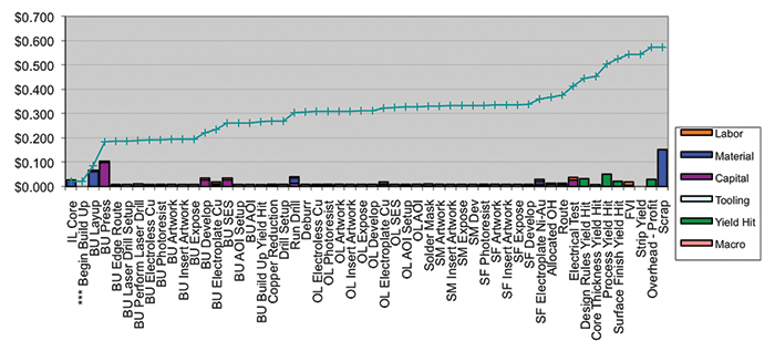
Figure 1. Example of activity-based cost modeling.
The innerlayer core and HDI buildup activities contribute significant material costs, as shown by the blue bars for those two steps. Any type of via drilling – laser or mechanical – will contribute capital costs since the throughput per panel is usually low. Many of the other activities contribute labor and equipment depreciation costs, as shown by the orange and purple bars.
Conductive Paste Interconnect
Conductive pastes are commonly used to make electronic interconnects and printed circuits. They come in several variations, ranging from nano-silver to epoxy-based metal fillers. They serve several markets and have been used in commercial and high-reliability applications. Most are air-cured formulations and may display a wide discrepancy in electrical resistance.
Conductive paste can be used in PCB fabrication as an alternative to copper-plated vias. Conductive paste vias are created by laser-drilling holes in a prepreg layer. A screen-printing process is used to fill these holes with conductive paste, and then the panel is heated and cured to sinter the paste. At this point the core with the conductive paste vias (Z-interconnect layer) can be included in the normal PCB layup and press lamination process.
Sintering is a process in which adjacent surfaces of metal powder particles are bonded by heating. Liquid phase sintering is a special form of sintering during which solid powder particles coexist with a liquid phase. Densification and homogenization of the mixture occur as the metals diffuse into one another and form new alloys and/or intermetallic species.
In transient liquid phase sintering (TLPS), compositions comprising powder metallurgy, a relatively low melting point (LMP) alloy and a relatively high melting point (HMP) metal are mixed in particulate form. At least one element within the alloy is either highly soluble in, or is reactive with, the receptive HMP metal. As the temperature is raised to the melting point of the LMP alloy, the alloy particles become molten. This transition can be observed as an endothermic event in differential scanning calorimetry (DSC). The reactive elements within the relatively low melting point alloy then react with the receptive high melting point metal to form new alloy compositions and/or intermetallic compounds. The formation of intermetallic species may be observed as an exothermic event using DSC. Thus, the typical TLPS DSC “signature” is an endotherm followed by an exothermic phase. The diffusion and reaction of the reactive elements from the LMP alloy and the receptive HMP metal continue until one of the reactants is fully depleted; there is no longer a molten phase at the process temperature, or the reaction is quenched by cooling. After cooling, subsequent temperature excursions (even beyond the original LMP alloy melt temperature) do not reproduce the original melt signature of the mixture. This is the “signature” of a typical low-temperature transient liquid phase sintered metal mixture.
Cost Modeling Results
As part of this project, the total costs of the following two scenarios were analyzed using the SavanSys activity-based cost modeling software described in the previous section.
Case 1 – Mobile phone board. This PCB uses a 10-layer HDI structure. The board is 2 x 2.5", and is similar in size and complexity to a smartphone motherboard. Using traditional HDI fabrication, this board would be a 4-2-4 structure – a two-layer core with four sequential buildup layers on the top and bottom. Using novel Z-interconnect technology, this board could be constructed using five cores and four Z-interconnect layers. The cross-section of each option is shown in FIGURE 2.
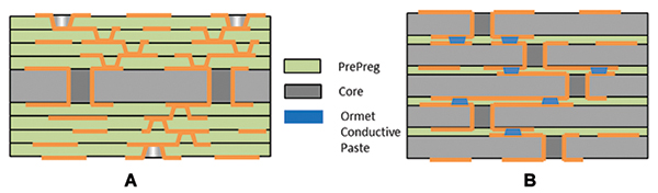
Figure 2. Cross-section of a 4-2-4 board (A) and a five-core Z-interconnect board (B).
The traditional HDI board is built by starting with a copper clad laminate core. The copper on this core is patterned on both sides, and through holes are drilled for the core vias. These through holes are plated to complete the core processing. Then, four HDI buildup processes are done, including lamination, laser drilling of the vias, imaging, and electroplating. These processes are done sequentially, and the board is completed with a surface finish and solder mask process.
The five-core Z-interconnect process uses five cores instead of one. Each core is fabricated using the same process as the core in the traditional HDI structure. However, instead of insulating each core using a solid sheet of prepreg, this prepreg is laminated and laser drilled to create core-to-core vias. These vias are filled with conductive paste to complete the core-to-core interconnect.
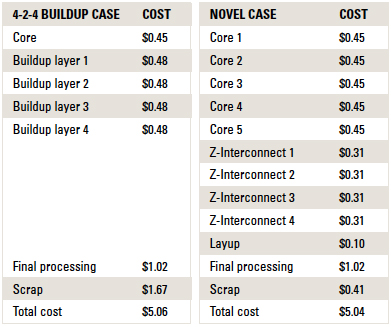
TABLE 1 shows the total cost of both options. The novel option is slightly less expensive, primarily due to the higher fabrication yields. For traditional HDI, each buildup layer introduces a cumulative yield loss that is combined with any prior yield losses. Conversely, each core in the novel case is processed in parallel instead of sequentially. Each core is thus tested in parallel instead of sequentially as well. Furthermore, the process to create the Z-Interconnect is a high-yield process, since
it only involves laser drilling through a prepreg screen printing of conductive paste.
Table 1. Cost Modeling Results
Case 2 – Large 28-layer server board. In this case, a 28-layer board is constructed using two cores made up of either 12 layers or 14 layers. The board is 15" by 20" (one board per panel) and 140 mils thick. All vias are 12 mil holes, and each core has a 90% yield. Using traditional PCB technology, the cores would be connected to each other using plated through hole (PTH) vias that extend all the way through both cores. However, another option is to use a Z-interconnect layer between the two cores to provide core-to-core connections. The cross sections of these two scenarios are shown in FIGURE 3.
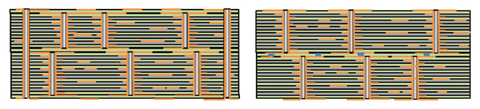
Figure 3. Drawing showing 28-layer board, the left with two cores connected with PTH and the right connector with with two cores connected with one novel Z-interconnect layer.
The following key cost and yield assumptions were used for this comparison:
- Each core can be 100% tested in the Z-interconnect case, but only 50% tested in the PTH case – The yield of the cores is the same for both cases, but since all the core-to-core interconnect is done through the Z-interconnect layer in the second case, the nets are all accessible for testing prior to lamination. However, when the core-to-core interconnect is done using PTH vias, all the nets are not routed to the surface. These nets cannot be tested until after final lamination.
- Outerlayer PTH drilling has a 10% yield loss – One of the major factors for PTH drilling yield loss is the aspect ratio of the vias. In this case, that aspect ratio is 11.67 (140 mil thick board and 12 mil PTH vias). That is a very high aspect ratio and could result in significant yield loss. In many cases, this yield loss can be minimized by using larger vias for the outerlayer interconnect. However, larger vias consume more board area, which may not be available in all cases.
TABLE 2 shows the cost of the Z-interconnect case to be lower than the conventional case based on the assumptions presented above.
Table 2. Cost Comparison of PTH Interconnect and Novel Z-Interconnect Interconnect
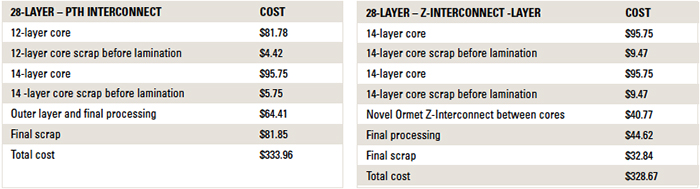
In both cases above, the cost of fabricating the cores is the same. A 14-layer core is assumed to cost $95.75 before any test and scrap, and the cost of a 12-layer core is $81.78. For the PTH via interconnect case, the construction of the final board is done using two outerlayers combined with a 12-layer core and a 14-layer core. One of the first differences apparent in the cost comparison is the difference in scrap cost before lamination. As described in the assumptions, one advantage of using the Z-interconnect layer to interconnect the core is the fact that all nets in the core are accessible for testing before final lamination. In the PTH case, many nets are not routed to the surface of the core and are therefore not available for testing until final lamination. This means there is less scrap before lamination, but there are undetected defects still in the cores that will cause additional scrap at the end of the process.
The other major difference in cost is the final scrap, which is due to a lower final yield in the PTH case. The lower final yield is due to residual defects in the core and high aspect ratio outerlayer drilling yield loss.
Summary
Use of a Z-interconnect layer with conductive paste vias is a cost-effective alternative to copper-plated microvias. The two cases analyzed showed that the addition of Z-Interconnect layers can be used to reduce total product cost. In both cases, this cost reduction was achieved through a variety of yield improvements as follows:
- When using Z-interconnect layers with conductive paste instead of copper-plated microvias (Case 1), the need for sequential buildup layers is eliminated. The example in here is a 4-2-4 structure requiring sour sequential lamination cycles compared to a single lamination cycle using Z-interconnect layers between five cores. Sequential lamination can cause significant yield loss, and therefore the avoidance of this improves final yield.
- When using Z-interconnect layers with conductive paste instead of PTH vias (Case 2), the final yield is improved by permitting more complete core testing before lamination and avoiding the need for high aspect ratio, low yield outerlayer through-hole drilling.
Ed.: This article was first published at IPC Apex 2014 and is republished here with permission of the authors.
Chet A. Palesko is president, Savansys Solutions (savansys.com); Amy J. Palesko is VP of business development, SavanSys Solutions; James Haley is vice president at Ormet Circuits (ormet circuits.com), and Catherine Shearer is senior scientist at Ormet Circuits; This email address is being protected from spambots. You need JavaScript enabled to view it..


