IPC-2152 is an important baseline for determining current carrying capacity, but further work must be done for individual applications.
In response to recent chatter about IPC-2152 in multiple online articles, I believed it necessary to reiterate the purpose behind the IPC design standard for sizing electrical traces.
IPC 1-10b is a task group of volunteers from several companies in the electronics industry. I was task group chairman from 1999 to 2016. We designed test boards and wrote IPC-2152, Standard for Determining Current-Carrying Capacity in Printed Board Design. The standard is intended to describe the test data used to define trace heating in a specific configuration through conductor sizing design charts. Testing was performed following IPC-TM-650, method 2.5.4.1A, “Conductor Temperature Rise Due to Current Changes in Conductors.” The design charts are only applicable to that configuration. Designs with different board sizes, thicknesses, and materials, including copper planes – when mounted by bolted fasteners or wedgelocks – have different trace temperatures for an applied current. People and corporations have to create their own charts if they want to have an accurate temperature for a given trace size and applied current. The information included in IPC-2152 provides that information. (Accurate temperatures can only occur from a design chart if that chart represents the specific technology.)
We created an appendix in IPC-2152 to help users understand a single design chart cannot be expected to describe the temperature rise of traces in all printed circuit board applications. Circuit boards vary in size and shape, have different dielectric materials, and vary in the number of layers and copper thicknesses, as well as mounting configurations.
It is not practical to perform current carrying tests to derive design charts that will be useful for all technologies. The intent of IPC-2152 is to provide enough information for companies to run their own testing or develop thermal models to determine conductor current carrying capacity in a given technology. Correlating a thermal model to IPC-2152 baseline data is a start. Correlating a thermal model to a known value validates the model. It is a practice to compare against a standard: in this case, IPC-2152.
The IPC-2152 Appendix includes baseline charts from test data for 0.5oz, 1oz, 2oz and 3oz copper internal conductors, as well as 2oz and 3oz external conductors. In addition, we included test results for testing in air and in a vacuum environment (space and high-altitude applications).
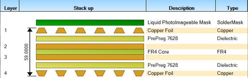
All this testing was performed with a polyimide test board that was 14" long, 7" wide and 0.07" thick. We tested the board suspended vertically and horizontally in still air for the air/Earth environments and suspended in a vacuum chamber for the space environments. No copper planes were in the board. The appendix includes measured thermal properties for the board materials we tested.
In the appendix, we included thermal modeling results to illustrate the temperature gradients around the traces in the polyimide test board while suspended in still air. The intention was to bring attention to the parallel conductor rule for sizing traces in proximity to each other. This rule is not practical. A better way to estimate the temperature rise for multiple conductors is to manage power and power density, although power and power density are meaningless without design charts that represent the technology.
We created many thermal models of printed circuit boards. The models were correlated to the test data with excellent results. We then used those thermal models to simulate the presence of copper planes. We varied the copper-plane thickness and the distance from the copper plane to the trace. Results showed what we expected: a significant drop in the trace temperature rise when the plane is close to the trace and not as much when the plane is moved away from the trace. We provided guidance regarding board size and the expected reduction in trace temperature when a full copper plane exists at a specific distance from the trace, but it was not followed up with any testing.
We wanted to include mounting configurations as well. We wanted to simulate bolted connections and wedgelocks, but we didn’t get to that. The mounting configurations will likely show a significant impact.
We collected trace heating data for FR-4 boards that were 14" long, 7" wide and 0.038" thick, as well as 0.059" thick. These data were not published. Models were created for these configurations, and charts were created for these boards with no copper planes, a 1oz copper plane 0.005" from the trace, and a 2oz copper plane 0.005" from the trace. We then expanded the data set of charts to include the configurations listed in TABLE 1.
Table 1. Unpublished Design Charts
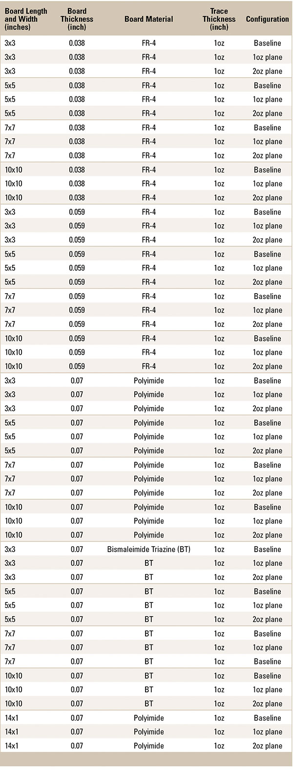
The configuration column represents three board configurations. The baseline has no copper planes. The 1oz plane designation represents a chart developed for when a single 1oz copper plane is included in the stackup that is 0.005" from the trace. The 2oz plane configuration is a chart with a 2oz copper plane that is 0.005" from the trace. We ran studies to investigate if the location of the internal trace (through the stack) had any significant impact on the temperature rise; it did not. We ran studies to see the impact of moving the trace to the edge; it did have an impact. We also ran studies varying the distance from the trace to the plane but didn’t develop charts from those studies.
Managing Currents and High-Power Densities
To educate users on IPC-2152 and its predecessor IPC-2221, I recently participated in a couple webinars and a HackChat. As a result of those appearances, I received a number of questions about managing currents up to 300A and managing high-power densities. For example, one student was designing a bridge rectifier with four Mosfets that each dissipated 15W of power and had a peak current of up to 80A. The student had questions regarding thermal vias and how to size them. I created a spreadsheet to calculate the thermal resistance through the board and estimate a temperature rise through the board for the power he was managing. I included a way to calculate the power losses in the conductors that were bringing in the 80A of current. In this particular design, the power was managed on the backside of the board. This design required handling 60W of power from the FETs and the conductor losses from the 80A through the board. This would be a challenge. We identified areas for him to concentrate on to improve the design.
When managing high current in any application, I start by looking at the power dissipated (I2R losses or Joule heating) by the conductors in addition to the components. It is easier to account for conductor losses in a thermal model for high current applications than rely on estimated temperature rise from the IPC-2221 or IPC-2152 design charts for two main reasons. The design charts don’t take into consideration copper planes or the mounting configuration. These two aspects have a significant impact on the thermal results in a PCB design. In addition, when we created the IPC design charts, our test data went only to 25A. Any calculations above 25A are an extrapolation. Small deviations or extrapolations of a few amps are reasonable, but up to 60A – and as much as 300A – require additional work. The charts are not valid for those applications.
The History of Conductor Sizing
Until publication of IPC-2152, people were using conductor sizing design charts published in IPC-D-275 and its successor, IPC-2221, Generic Standard on PCB Design. Those charts were the source of motivation to create IPC-2152. It took a few years (1998 to 2000) before we understood no one had actually collected and published internal trace heating data before. This was a revelation since there was a design chart for internal conductors (traces) in IPC-2221.
At some point, when multilayer boards were being constructed, a decision was made to create an internal trace heating chart. The internal chart shows up in the MIL-STD-275E standard that preceded IPC-D-275, which eventually became IPC-2221. The internal trace sizing chart was defined by using half the current from the external trace chart, not from test data. The logic behind that choice was never documented.
The IPC-2221 external trace sizing chart originated from work at the National Bureau of Standards from 1954-56. Several reports describe the efforts used to define the electrical characteristics of printed circuits and the dielectrics. Current carrying capacity was documented in NBS Report 4283. The first design chart was for external traces because they had only two-sided boards then (FIGURE 1). (Notice the word “Tentative.”)
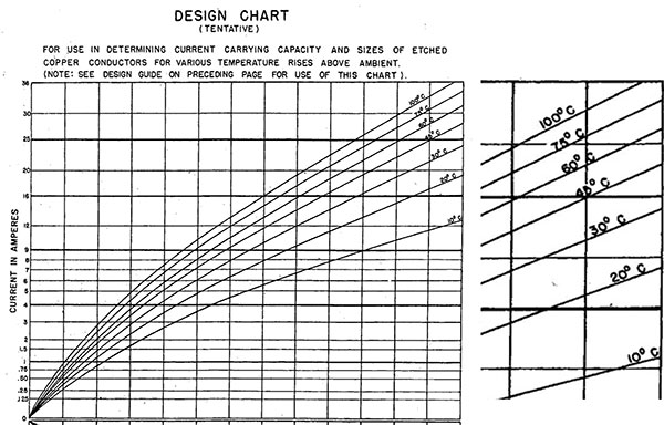
Figure 1. Tentative NBS chart.
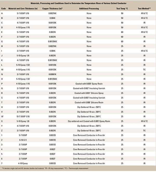
TABLE 2 describes the datasets that went into creating that chart. The overall dataset results in a mix of variables that impact trace temperature rise include different board materials, different board thicknesses, and different board widths – as well as without copper planes. Board material, board thickness, and the presence of copper planes all have a major impact on the resulting trace temperature rise. A design chart comprised of a mix of variables used to assess the current carrying capacity of an external trace is misleading.
Table 2. NBS Data for External Conductor Sizing
Each line of constant temperature rise in Figure 1 represents a dataset. Each data point in the set represents the amount of current required to raise given size traces to 10°C, or the temperature level for the specific curve (10°C up to 100°C). These data points were graphed by hand on log paper, and a French curve was likely used to define what was considered a best fit.
Table 2 contains a list of all the boards tested to create these design curves. There are four groupings. The group of boards used to create the curve for the final chart is from those labeled “None” in the additional processing column.
Many engineers did principal hand calculations, as well as computer modeling, in an effort to obtain results to match these curves. Not knowing where the data came from made it impossible to obtain a reasonable correlation, especially for the internal conductor sizing charts. (This is why we included as much information as possible in the IPC-2152 Appendix.)
The list of NBS boards includes different dielectric materials: phenolic (XXXP), epoxy and G5. The boards varied in thickness: 1/32 (0.0312", 0.793mm), 1/16 (0.0625", 1.588mm), and 1/8 (0.125", 3.175mm). Some boards had copper planes on the backside.
The boards with copper planes are of interest because they show the variance in current level for a given Delta T as a function of the distance from trace to a copper plane.
Either thermocouple or the IR drop method measured the trace temperature rise. The IR drop method is best. They tested 1oz, 2oz and 3oz copper traces, some with coatings and some stripped completely off the board. The traces stripped from the board are my favorites.
Ironically – or perhaps by design – the traces stripped from the board and tested in air come close to matching the IPC-2221 internal conductor sizing chart. A lot of information in that data aids understanding trace heating and validates the studies performed to develop IPC-2152.
The NBS 20°C rise curve data set is shown in FIGURE 2. It shows the variation in current level for a given cross-sectional area and the resulting 20°C temperature rise.
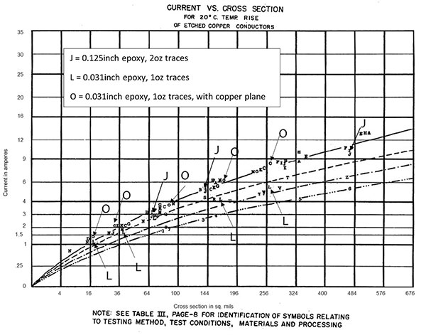
Figure 2. 20°C rise curve.
Technology-Specific Design Charts
Accurate design charts, incorporated in an easy-to-use software application, are one step toward a better predesign process for sizing electrical traces. As the industry becomes educated in the fundamentals of heat transfer, it will become obvious design charts that match a technology add more functionality than what we see today.
Many PCB design issues are unsolved. Vias aren’t difficult to assess until multiple vias are used to pass current from one layer to another. If the vias do not share current equally, the design is more complex.
Flex circuits are essentially thin boards, some with copper planes and some without. I recommend the old internal trace sizing chart for flex without copper planes. When multiple-layer flex is made and the layers are booked, that becomes a really different problem. I like seeing the conductors sized to minimize the power loss. Calculating total power loss in the flex circuits assesses the thermal design.
Wagon wheels and neckdown areas can also be assessed by using power and power density as a criterion for assessing thermal limitations. Accurate temperature assessments can only happen with charts that represent the technology.
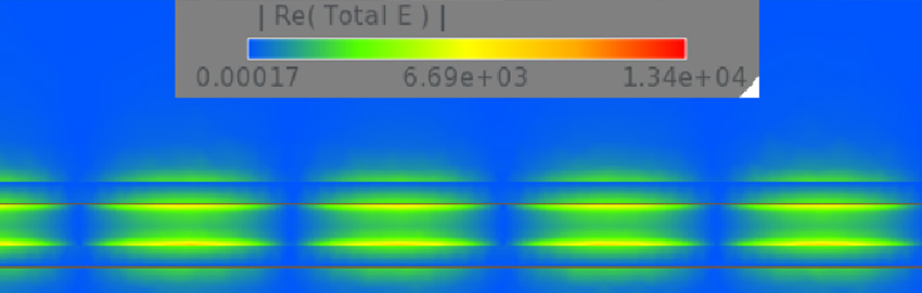
Another great use of technology-specific design charts (TSDC) and design criteria based on power and power density (to estimate trace temperature rise) is managing parallel conductors. Parallel conductors are traces running current at the same time, all closely spaced side by side and in the stackup.
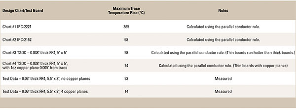
Testing should be performed to understand all the aforementioned items. Parallel conductors are an area we accomplished some testing. The parallel conductor test measured seven 10-mil traces spaced 10 mils apart, all running 1A. Two boards were tested, one with no copper planes and one with four 1oz planes evenly spaced in the stackup. Both boards were 5.5" wide, 8" long and 0.06" thick. The traces were 1oz and were calculated to be 0.001" thick when 10 mils wide. (A resistance measurement is made with low current. Using the resistance and length of the trace, the cross-sectional area can be calculated. We did not get coupons.)
Parallel Conductor Test Results
Let’s examine the temperature rise of the seven parallel traces. Seven 10-mil traces are spaced 10 mils apart, 0.001" thick, all running 1A. TABLE 3 shows the results.
Table 3. Design Chart vs. Test Data
Conclusion
Many conductor issues in the predesign phase, aside from trace temperatures, become apparent after the board is made. Understanding conductor temperature rise for micro technology, as well as managing 300A of continuous current, can be a key element to successful designs. Thermal analysis and testing do a reasonable job of evaluating the end results, but it would minimize respins if we were a little closer in our predesign phase of printed circuit design.
Creating conductor sizing design charts for a given technology provides many insights that clear up old rules of thumb and the fallacy of internal traces running hotter than external traces. Many areas of design could benefit from better conductor design charts. IPC-2152 has all the information needed to make your own technology-specific design charts.
Mike Jouppi, recently retired, spent his career as a thermal analyst. At Lockheed Martin, he performed thermal analysis of electronics used on spacecraft and space systems; This email address is being protected from spambots. You need JavaScript enabled to view it..