Stop designing products guaranteed to fail EMC testing.
Au: This article emphasizes the need to concentrate on design of transmission lines, or the “spaces,” instead of the “wires.” The industry focus has been on the movement of charges in the wires, which only occurs because the electric fields are moving. The energy is carried by the fields, not the displacement current. My apologies to the EM physicists for oversimplifying these concepts, but this approach will increase the chances of success for most designs.
Engineering teams worldwide are facing increasingly difficult challenges to design electronic products and achieve good signal integrity and compliance. However, the status quo is to expect the design to fail EMC testing not once, but three, four, or as many as five times. Each time the design is sent to be retested, there is little confidence in success. This cycle is expensive in both the time it takes to redesign the product and the cost of expediting fabricating the new PCB and assembly. Add this to the cost of retesting the product, and the numbers add up very quickly. This expense and delay in product certification are not in the budget or the schedule. The cost not only directly affects the bottom line of the electronic supply company, but also affects the customers waiting for the product. Instead of designing the next big thing, teams are trying to fix the current one. As a result, billions of dollars are lost each year designing products that are expected to fail.
What is wrong here? The billion-dollar mistake.
The billion-dollar mistake is rooted in the misunderstanding of the nature of electronic energy. One drawing is to blame.
FIGURE 1 shows a battery connected by wires to a light bulb. The arrows are supposed to show current flow. From this, the wires started to be called “conductors,” since the energy flowed in the wires. The current flowed in a loop, so the idea this was a circuit was born. If this were true, then as soon as the switch was closed, the energy would be instantly seen at the load, and there would be no such things as signal integrity or EMC problems. There would also be no such thing as radio because the energy is the same in an electrical system or air. There would also not be any life on earth, as light from the sun would not travel here without the wires.
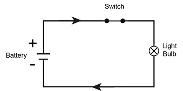
Figure 1. Is this how current really flows?
The perspective from this simple drawing has set the tone and philosophy for PCB design. The focus has been on current flowing in the conductor. The result has been a steady increase in failure to pass EMC requirements as the IC geometries grew smaller and switching frequencies increased.
Why did this happen? Recall the scenario of a frog in a pan of water. As the water temperature rises, the frog does not notice until it is too late. The electronics industry behaves much the same way, to its detriment. This incorrect perspective now costs the industry billions of dollars every year.
Ralph Morrison taught me the importance of language. In this case, incorrect language set the stage for bad design practices. It became the norm to design the conductors, connecting the battery or power source to the load. As long as the speed of the switch was relatively slow, this appeared to be the correct path. For earlier devices, this perspective was not so bad that it caused failures, but it has led to the creation of design rules that make it increasingly difficult to pass certification.
The Real Picture
The wires are not the primary energy conductors; they form boundaries, much like the banks of a stream. The main energy does not flow through the wires; it travels through the space between the wires. This space, or dielectric, is the primary conductor. The energy is carried by the moving EM fields in the dielectric, not electron flow in the wires. Proper perspective for current flow is the amount of field moving past a point in the transmission line.
Field stored in the left side does not move (FIGURE 2a). As the switch starts to close, the field starts to move (FIGURE 2b). The switch is closed, so the field moves into the new space (FIGURE 2c). The switch is open, so the field stops moving from the left (FIGURE 2d).
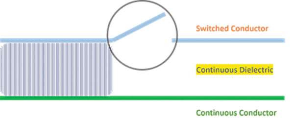
Figure 2a. Field behavior in four steps. Field stored in the left side does not move.
Figure 2b. As the switch starts to close, the field starts to move.
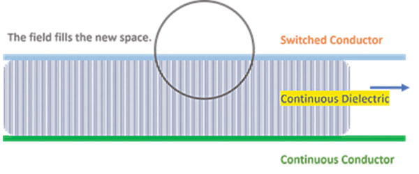
Figure 2c. The switch is closed, so the field moves into the new space.
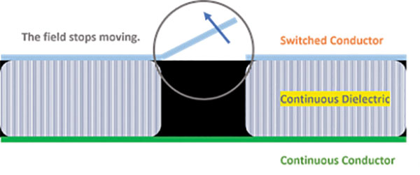
Figure 2d. The switch is open, so the field stops moving from the left.
Field behavior is simple to understand. When stored between two conductors, separated by a dielectric, the field stays put. Once the switch is closed, the field moves sequentially into the new space, like water moving into a hose from a faucet. Once the switch is opened, the field from the source stops moving because the two spaces are no longer connected. The field behavior after the switch is determined by what is at the other end of the space.
Simple rules of triplets can explain field control (FIGURE 3). You need three things to store field: two conductors separated by a dielectric. Electronic systems have only three types of components: conductors, dielectrics and switches. You can only do three things with electromagnetic field: store it, move it, or convert it into kinetic energy.
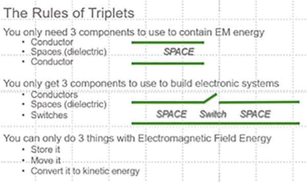
Figure 3. The rule of triplets.
This misconception has led to design practices that almost guarantee failure. The cost to the industry is staggering. When a typical project fails EMC testing, it has to be redesigned, remanufactured and retested under pressure to get it done quickly. These redesign cycles usually involve minimal changes, and the results are often disappointing. The cost can range from tens of thousands to hundreds of thousands of dollars, and weeks to months of delay. There is typically no budget for either the funds or the time, and the impact on the business is huge.
Imagine this on a global scale: thousands of design teams spending time and money redesigning products instead of working on new ones, all because of a simple mistake in language.
To call this a billion-dollar mistake is an understatement.
Daniel Beeker is senior principal engineer, automotive field applications engineering, NXP Semiconductors (nxp.com); This email address is being protected from spambots. You need JavaScript enabled to view it..


