Contact lenses that can monitor your health as well as correct your eyesight aren’t science fiction, but an efficient manufacturing method – finding a way to produce the curved lenses with embedded electronics – has remained elusive.
Until now. A team of researchers from the University of Houston and the University of Colorado Boulder has reported developing a new manufacturing method, known as conformal additive stamp printing, or CAS printing, to produce the lenses, solar cells and other three-dimensional curvy electronics. The work, reported in the journal Nature Electronics, demonstrates the use of the manufacturing technique to produce a number of curvy devices not suited to current production methods. The work is also highlighted by the journal Nature.
“We tested a number of existing techniques to see if they were appropriate for manufacturing curvy electronics,” said Cunjiang Yu, Bill D. Cook Associate Professor of Mechanical Engineering at the University of Houston and corresponding author on the paper. “The answer is no. They all had limitations and problems.”
Instead, Yu, who is also a principal investigator with the Texas Center for Superconductivity at UH, and his team devised a new method, which they report opens the door to the efficient production of a range of curvy electronic devices, from wearables to optoelectronics, telecommunications and biomedical applications.
“Electronic devices are typically manufactured in planar layouts, but many emerging applications, from optoelectronics to wearables, require three-dimensional curvy structures,” the researchers wrote. “However, the fabrication of such structures has proved challenging due, in particular, to the lack of an effective manufacturing technology.”
Existing manufacturing technologies, including microfabrication, don’t work for curved, three-dimensional electronics because they are inherently designed to produce two-dimensional, flat electronic devices, Yu said. But increasingly, there is a need for electronic devices that require curvy, 3-D shapes, including smart contact lenses, curved imagers, electronic antennas and hemispherical solar cells, among other devices.
These devices are small – ranging in size from millimeters to centimeters – with accuracy within a few microns.
Recognizing that, Yu and the other researchers proposed the new fabrication method, conformal additive stamp printing, or CAS printing.
CAS printing works like this: An elastomeric, or stretchy, balloon is inflated and coated with a sticky substance. It is then used as a stamping medium, pushing down on pre-fabricated electronic devices to pick up the electronics and then print them onto various curvy surfaces. In the paper, the researchers describe using the method to create a variety of curvy devices, including silicon pellets, photodetector arrays, small antennas, hemispherical solar cells and smart contact lenses.
The work was performed using a manual version of the CAS printer, although the researchers also designed an automated version. Yu said that will make it easy to scale up production.
In addition to Yu, co-authors include Kyoseung Sim, Song Chen, Zhoulyu Rao, Jingshen Liu, Yuntao Lu, Seonmin Jang, Faheem Ershad and Ji Chen, all with UH, and Zhengwei Li and Jianliang Xiao, both with the University of Colorado Boulder.
This work was supported by National Science Foundation.
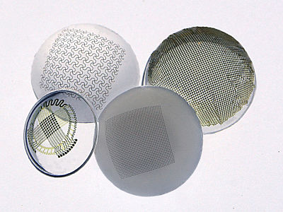
Figure 1. A team of researchers led by University of Houston engineer Cunjiang Yu has reported a new way to manufacture curvy, three-dimensional electronics.


