A newly developed treatment technology for copper foil enables ultra-low profile surfaces.
Subtractive and semi-additive processes are widely used for circuit pattern formation in high-volume PWB manufacturing. In a subtractive process, copper is removed from an entirely copper-laminated board to expose the wiring pattern. Dry-film resist is applied as an etching resist. The dry film is exposed, and then developed, which removes the unexposed parts. When resist is stripped, copper traces appear. The advantage of the subtractive process is its (low) cost and excellent mass producibility.
In semi-additive processing, the wiring pattern is electroplated onto a copper layer. A dry-film resist is applied as a plating resist. Unlike a subtractive process, the negative/positive part of the resist is reversed. Additional copper is plated on the unmasked areas. Then the dry-film resist is stripped away, and a brief etching step removes the exposed thin copper layer from the board. The advantage of the semi-additive process is it can provide finer lines than subtractive processes. To improve plating adhesion, a desmear treatment is used by modifying the resin surface roughness. It seems there is difficulty removing contamination from electroless plating on the desmear surface. FIGURE 1 illustrates the process comparison of subtractive and semi-additive processes.
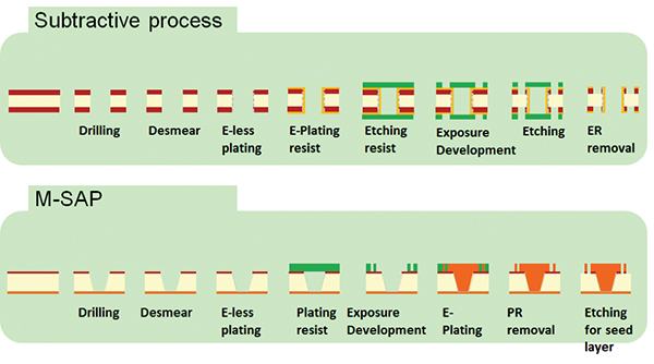
Figure 1. Manufacturing process comparison of subtractive and semi-additive processes.
Conventional copper foil. Two types of copper foils are used in PCBs1: ED (electrodeposited) and RA (rolled annealed). The most common foil used in PCBs is ED. ED foil is produced through an electrochemical process. As ED foil is formed, the rotation speed determines the resulting foil thickness. Typically, copper is plated on a cylindrical drum. Then, the smooth surface (shiny side) is achieved from drum side. Better coplanarity and less wave undulation is achieved on the drum side. Topological modification is widely used by plating copper to increase the surface area. Nodules are formed on the outer surface of the copper foil.
When nodules are formed on the drum side of the copper foil (called reverse-treated foil), it is easier to maintain the profile of copper. The advantage of nodule formation is improved adhesion, thanks to a strong anchoring effect. This is needed to meet reliability requirements. The rough surface is called the matte side.
FIGURE 2 compares surfaces of shiny and matte sides. Various sizes of nodules are available for various applications; FIGURE 3 demonstrates this by means of top and cross-sectional views. Then additional plating is applied over the nodules for thermal barriers using zinc, nickel, etc. Anti-rust agents or adhesion promoters are also applied to the surface of nodules. These improve the copper foil’s adhesion and tarnish properties. These coatings can prevent reductions in adhesiveness after thermal or chemical degradation through the PCB assembly process as well.
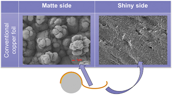
Figure 2. SEM images for surface comparison.
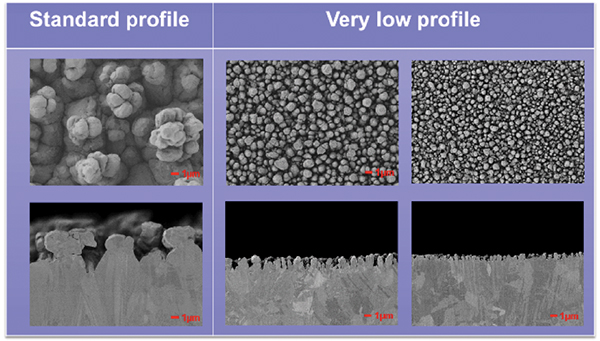
Figure 3. SEM images for profile comparison.
Nanoscale profile copper foil. The profile size of copper foil has become a more important consideration for PCBs. The smaller profile size is a key factor in next-generation PCBs. In terms of fine pattern formation, copper foil surface roughness is a key factor for improving etching behavior. From an electrical point of view, a flat surface is desired for high-speed applications with high-frequency signals.
A nanoscale profile copper foil has been developed, which shows well-balanced etching capability and adhesion. An acid cleaning process removes the oxidized copper layer prior treatment (FIGURE 4, left). Nanoscale nodules are formed on the copper surface by chemical reaction using a proprietary treatment solution (Figure 4, right). Then the surface of copper foil is covered with a uniform and dense layer. The nanoscale nodules have a large contact area that offers secure bonding to prepreg by means of the anchoring effect. Scanning probe microscope (SPM) images are shown in FIGURE 5. For the conventional very-low profile copper foil, the SPM images are similar to SEM images. However, SPM shows a quite different image of nanoscale profile copper foil. It seems probes have difficulty tracing the sharp nano surface.
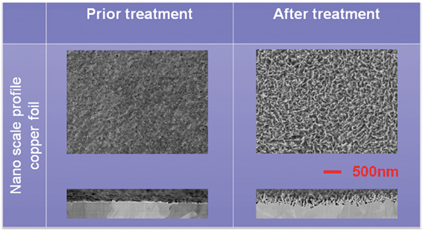
Figure 4. SEM images for morphology of nanoscale noduled copper foil.
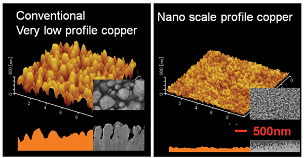
Figure 5. SPM images for morphology comparison.
Fine line capability. The nodule of copper foil is embedded in the prepreg as it is subjected to hot press lamination. In the case of a subtractive process using conventional copper foil, it has to be etched completely because the large-size nodules get stuck in the prepreg. This may cause over-etching of the wiring pattern. FIGURE 6 shows 3D images from a confocal microscope of 9µm thick copper foil and nanoscale foil. The nanoscale profile copper has twice the etch factor (TABLE 1). The surfaces of prepreg and the anchored part of copper are completely different in appearance. SEM images comparing etching characteristics of a copper foil profile are shown in FIGURE 7.
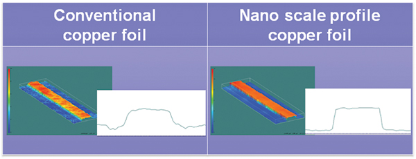
Figure 6. 3D images for trace after etching.
Table 1. Etch Factor
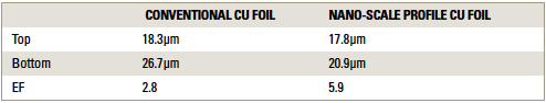
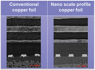
Figure 7. SEM images for the comparison of fine line formation.
Adhesion behavior. Peel strength is performed with 30µm thick specimens by performing additional copper plating. The prepreg of FR-4 was laminated with copper foil. Results are shown in FIGURE 8. There is no significant difference between the 9µm and 18µm thick copper foil with nanoscale profile copper. The adhesion strength is acceptable on both copper foils. The nanoscale profile copper foil demonstrated 20 to 30% lower peel strength than the conventional copper foil. The samples showed different fracture behavior, even though they shared the same adhesion failure. The fracture location of nanoscale profile copper is close to the copper surface (FIGURE 9). The surface of nanoscale copper foil is covered with resin of prepreg (FIGURE 10).
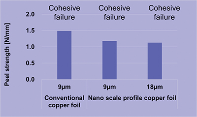
Figure 8. Result of peel strength.
Figure 9. Fracture location after peel test.
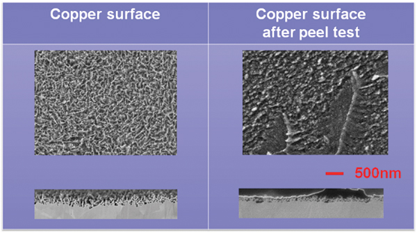
Figure 10. Fracture surface after peel test of nanoscale profile copper foil.
Finite element simulations. To address this behavior of nanoscale copper foil, FEM (finite element modeling) was used for stress analysis. The maximum principal stress was conducted. Typically copper foil is laminated with prepreg or buildup material at high temperature. The maximum principal stress is conducted by calculation of the accumulated principal stress at -55°C using Ansys 16.1 software. Prepreg and copper foil are contained in the model. The material supplier describes typical properties of the prepreg. It is overall property of prepreg, but it is not localized property. Segmented, accurate parameters are required for prepreg. Prepreg material is a mixture of glass fabric, resin and filler. The glass fabric layer and resin/filler layer are separated. Filler is distributed in the resin.
Filler volume information was extracted from a cross-sectioned SEM image. The image-processing algorithm is outlined in FIGURE 11. The SEM image was split into 500nm thick images for resin filler layer of prepreg. Binary images were generated, which highlighted the filler parts (in green) within the selected region. The filler defines the shape of the target. FIGURE 12 shows the binary image obtained from the contrast-enhanced image. The volume of filler is calculated on each tomographic image. CTE (coefficient of thermal expansion) and modulus are conducted by a curve-fitting technique based on filler volume information. Then, segmented model parameters for prepreg are conducted. The parameters of FR-4 type prepreg are shown in FIGURE 13. A localized realistic model of copper foil is implemented in this study for FEM, which can recognize the nano-structure with representative prepreg.
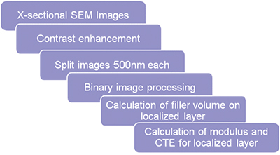
Figure 11. The image-processing algorithm.
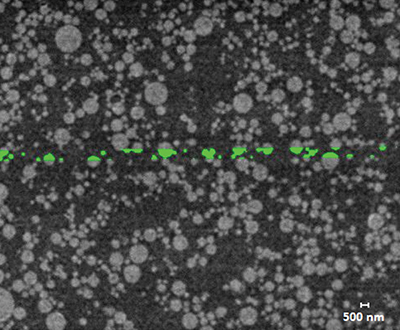
Figure 12. Binary image processing for filler distribution in prepreg.
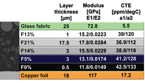
Figure 13. Segmentalized property of prepreg for FR-4 type prepreg.
Localized realistic model for nanoscale profile copper. The simulation model used a 1 to 4µm size nodule with a simplified conventional profile (FIGURE 14). Given the adhesion results, higher maximum principal stress is expected on nanoscale copper foil. Simulation results are shown in FIGURE 15. Simplified nanoscale profile is flat model, resulting in low stress distribution, as indicated. The maximum principal stress of conventional foil is greater than that of the nanoscale profile copper. These results contradict the adhesion test results. Macro size simulation model does not match nanoscale profile.
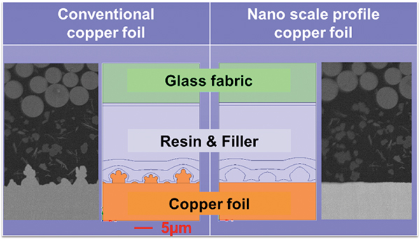
Figure 14. Simplified model.
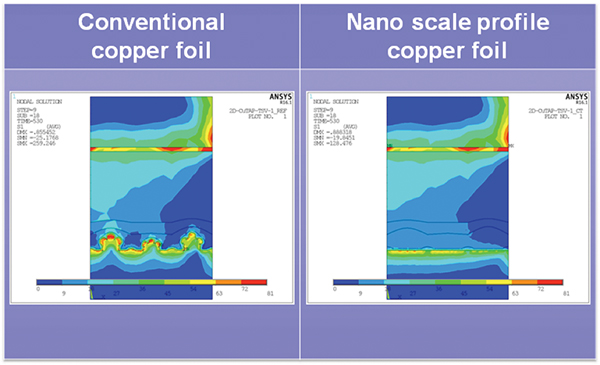
Figure 15. Maximum principal stress of simplified model.
The localized realistic model is proposed in FIGURE 16. The result of the maximum principal stress on FR-4 is shown in FIGURE 17. Higher stress level is conducted on nanoscale profile copper. This seems reasonable for adhesion test. The result on BT and buildup film is shown in FIGURE 18. Almost the same level of maximum principal stress is achieved on BT on both foils, which is quite low, because BT has unique characteristics such as low CTE and high Tg. FIGURE 19 shows the results of the comparison of segmentalized parameter and typical parameter. Results were different based on the prepreg. In the case of buildup film, no glass fabric was incorporated, resulting in similar parameters used. The segmentalized parameter is closer to the real situation. As such, the results should be more accurate.
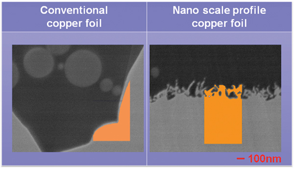
Figure 16. Localized realistic model.
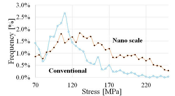
Figure 17. Maximum principal stress (FR-4) of localized realistic model.
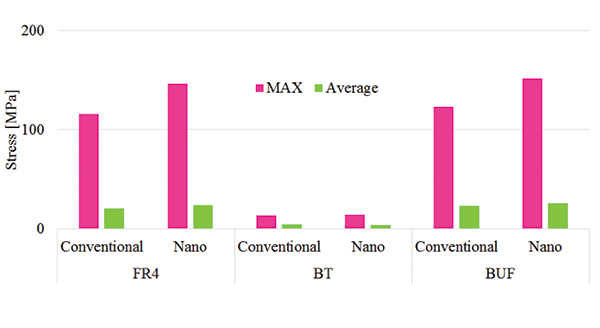
Figure 18. Comparison of maximum principal stress.
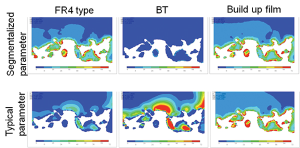
Figure 19. Comparison of parameter of prepreg.
Conclusion
A newly developed nanoscale profile copper foil is introduced as ultra-low profile copper foil for PCBs fabricated using subtractive processes. Fine-line capability is demonstrated, and it seems 20-25µm traces are possible using a subtractive process. This would contribute to a reduction in cost. Good adhesion is confirmed even though the surface is flat. Adhesion behavior was investigated through simulation. A localized realistic model and segmentalized parameter of prepreg are important to calculate the accumulated principal stress at the nanoscale level. The use of nanoscale profile copper foil is highly recommended for fine-line PCBs using a subtractive process.
Acknowledgments
The authors would like to thank KTT Inc. for kind advice and further evaluation.
References
1. JEITA, Japan Jisso Technology Roadmap, 2015 Edition.
2. J.U. Knickerbocker, et al, “2.5D and 3D Technology Challenges and Test Vehicle Demonstrations,” Proceedings of the 62nd Electronic Components and Technology Conference (ECTC), May 2012.
3. J.H. Lau, “TSV Manufacturing Yield and Hidden Costs for 3D IC Integration,” Proceedings of the 60th Electronic Components and Technology Conference (ECTC), May 2010.
4. K.W. Lee, et al, “A Resilient 3-D Stacked Multicore Processor Fabricated Using Die-Level 3-D Integration and Backside TSV Technologies,” Proceedings of the 64th Electronic Components and Technology Conference (ECTC), May 2014.
5. Y.H. Hu, et al, “Process Development to Enable 3D IC Multi-Tier Die Bond for 20m Pitch and Beyond,” Proceedings of the 64th Electronic Components and Technology Conference (ECTC), May 2014.
6. T. Kanki, et al, “Development of highly reliable Cu wiring of L/S=1/1μm for chip to chip interconnection,” Proceedings of the 2012 IEEE International Interconnect Technology Conference (IITC), 2012.
7. K. Oi, et al, “Development of New 2.5D Package with Novel Integrated Organic Interposer Substrate with Ultra-fine Wiring and High Density Bumps,” Proceedings of the 64th Electronic Components and Technology Conference (ECTC), May 2014.
8. H. Noma, et al, “HAST failure investigation on ultra-high density lines for 2.1D packages,” Proceedings of the International Conference on Electronics Packaging and IMAPS All Asia Conference (ICEP-IAAC), 2015.
Ed.: This article was first published at the SMTA Pan Pacific Microelectronics Symposium (Pan Pacific), January 2016, and is republished with permission of the authors.
Osamu Suzuki, Akito Yoshii, Hironobu Tsubura, Makiko Sato, Naoki Obata and Yoshinobu Kokaji are with Namics Corp. (namics.co.jp); This email address is being protected from spambots. You need JavaScript enabled to view it..


