
The stack-up and materials are the backbone of a board design.
I’ve been searching for a reasonably solid, fairly-simple approach to selecting laminates for a good part of the last eight years. (This was a background task to marketing laminates and designing software for stack-up design and material selection.) I’m writing about this now because I think enough water has gone under the bridge to where I’ve landed on a somewhat useful answer.
During my quest, I’ve probably been involved in 100 or more material-selection decisions, and my radar has been up for some sort of decision tree that would help. I found one such map dated July 2009, but it didn’t quite make sense to me, and no one had updated it in the decade that followed. The variables made sense; the decision tree didn’t.
For epoxy-glass laminates – excluding polyimide materials and PTFEs – the universe of current material choices looks a good bit like FIGURE 1 below. (A bit overwhelming.)
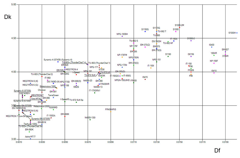
Figure 1. Big list of materials reporting Df vs. Dk at 1GHz. (Z-planner Material Mapper, using data from laminate manufacturers)
Assumptions. I’m intentionally going to withhold a few important parameters from the present discussion: 1) whether a material meets UL halogen-free requirements, 2) detailed reliability testing on actual test vehicles, and 3) price. My assumption is you already know whether halogen-free requirements need to be met, and price is beyond the scope of this column. Detailed reliability testing is a standalone topic for one or more columns. And, as mentioned, I’m narrowing the scope to exclude polyimides and PTFE materials for a separate discussion.
Board thickness. The thicker the board, the more you need to worry about stresses in the z-direction during soldering processes. Since boards are exposed to thermal excursions that exceed 225°C with today’s lead-free solder, PCB materials with the most significant thermal expansion are going to be a significant failure concern. The thicker the board, the more you’ll want to lean toward high glass-transition temperature (Tg) materials, and toward materials with comparatively-low z-CTEs (coefficients of thermal expansion in ppm/°C.) FIGURE 2 shows various board thicknesses and some rule-of-thumb recommendations for Tg. When designing thinner boards, mid-Tg materials can save about 25% or more on materials costs, particularly important in high-volume production.
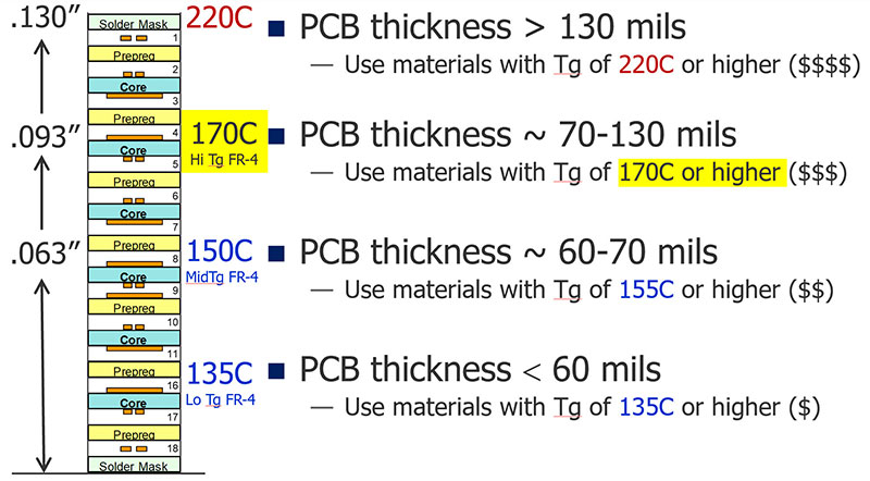
Figure 2. Board thickness and Tg.
Note the fabricator(s) may or may not make this distinction. If they have UL certification for predominantly high-Tg materials, that’s what you’ll have to live with unless you shop around.
Here, we’ve narrowed our material search a good bit, assuming you want to optimize for cost. Next, we’ll focus briefly on electrical parameters with an eye toward simplifying the discussion to some basic heuristics. (Detailed insertion-loss analysis is beyond the scope of this particular column.) From here, I’ll primarily focus on high-Tg materials for today’s high-layer count, higher-speed digital PCB designs.
Electrical parameters. Similar to golf scores, lower is better for Dk (dielectric constant) and Df (dissipation factor or loss tangent). Low Dk is better for crosstalk and for making the board as thin as possible. Typical high-layer count, high-Tg laminates have Dks in the 3.3-4.0 range.
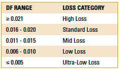
The more sophisticated OEMs and fabricators tend to categorize laminates from a Df into five major groups, typically at 10GHz: high loss, standard loss, mid loss, low loss and ultra-low loss. These are shown in TABLE 1. The values shown are typically reported at 10GHz. Note that precision for Df beyond three digits is usually artificial. Few have measurement equipment with that resolution.
Table 1. Typical Df/Loss Buckets for High-Layer-Count Laminates
If you’re designing a board in the 110 mil range, let’s say you want to consider materials with a Tg between 170° and 200°C, for example. And let’s say we’re targeting materials in the “low loss” range. That narrows the scope from Figure 1 to what is shown in FIGURE 3.
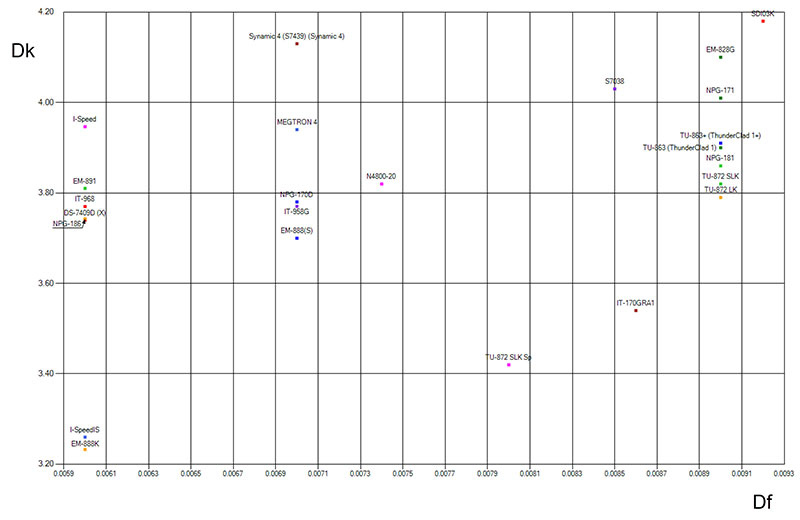
Figure 3. Narrowed list of materials, including materials with Tg from 170°-200°C, with self-reported Df values in the low-loss range at 10GHz. (Z-planner Material Mapper, using data from laminate manufacturers)
If you know where you need to be from a loss-category standpoint and the board thickness, you’ll have narrowed the list of possible materials considerably. (Notwithstanding UL certification at your current fabricators, also beyond the scope of this column.) In fact, you’ll be several steps ahead of design teams who just toss designs over the wall to their fabs to ask for recommendations. Since stack-up decisions and materials are the backbone of a board design, it would serve us all well to become savvier consumers, for electrical reasons in addition to mechanical reasons and cost control.
Parting thoughts. It’s likely we’ll want to narrow our search a good bit beyond the list in Figure 3. Next month, I’ll talk about how to narrow our list to maybe three materials we want to take a closer look at.
Bill Hargin has more than 20 years’ experience in PCB design software and materials. He is director of everything at Z-zero (z-zero.com); This email address is being protected from spambots. You need JavaScript enabled to view it..


