
RLC modeling has fundamental importance.
Creating equivalent electrical models for PCB interconnects utilizing ideal resistors, inductors and capacitors is important for both time and frequency domain analyses.
Figure 1 presents equivalent circuits for transmission lines, vias, connectors and decoupling capacitors1. Interconnect elements such as IC packages2 and sockets can also be modeled with lumped RLC components.
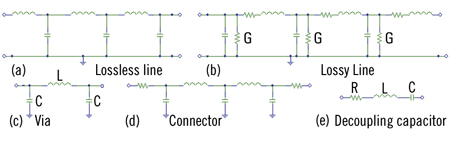
FIGURE 1. RLC models for several PCB entities: (a) lossless transmission line, (b) lossy line, (c) via, (d) connector and (e) decoupling capacitor.
|
Figure 1a depicts a 3-section lumped-circuit representation for a lossless line. Generally, when modeling a line using n-LC sections, the L for each section can be ascertained by dividing the total line inductance (equal to product of line delay TD and line characteristic impedance Z0) by number of cells n. C of each section can be calculated by dividing total line capacitance (equal to TD/Z0) by n.
The general lossy line, which accounts for frequency dependent skin effect R α √ f and dielectric loss G α f, is called RLGC model (Figure 2b). Only single net (uncoupled) cases are shown by Figure 1; however, coupled interconnect models can be also constructed using R, L and C components.
A topology consisting of a driver, interconnects and receivers may be represented by an equivalent circuit with a voltage source connected to an RLC network. This is because the driver IC can be modeled as a voltage source and a series resistor3. The receiver ICs can be modeled as capacitors, and interconnects as combination of ideal resistors, capacitors and inductors.
RLC models have frequency/rise time limitations. For sufficient accuracy4 a structure should be divided into model segments correlating to lengths of λ /20, Tr/10 or T_mrg/10. Where, λ corresponds to wavelength of highest transmitted frequency, Tr represents rise time and T_mrg is desired timing margin.
At frequencies/speeds beyond limits of lumped modeling, interconnect structures can be modeled using distributed techniques or S-parameters Touchstone files. The S-parameter matrices offer some attractive features such as eliminating fixture effects5. However, they are more difficult and restricted, compared to RLC models, for SPICE simulations. Also, S-parameter models require evaluation for passivity, causality5 and sometimes for symmetry (i.e., S12 = S21, S32 = S23, etc.).
RLC modeling of interconnects carries fundamental significance in spite of its limitations. RLC models are compatible with SPICE (and numerous other simulator programs), and can be created via several methodologies, including analytical/numerical, time and frequency domain measurements. A comprehensive overview of such electrical characterization techniques has been recently published6.
There are numerous equations governing RLC circuits, some of which are listed in Table 1.
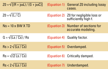
Table 1. A set of formulae for RLC networks.
|
In Equations 1 and 2 of the table, R, L, G and C represent series resistance, series inductance, shunt conductance and shunt capacitance7 of the transmission line, respectively. The angular frequency ϖ is related to cyclical frequency f via ϖ = 2πf.
Equation 1 is a general formula, including lossy cases, for transmission line impedance (Z0). Equation 2 defines Z0 for negligible losses, or sufficiently high frequencies (i.e., R << ϖL, and G << ϖC). In Equation 3, Ns is the minimum required number of LC sections for accurate modeling of a line with time delay TD. It indicates8 that for delay TD, at least Ns cells are needed to achieve bandwidth BW - the largest sine-wave-frequency component for which the model accurately predicts behavior of the actual modeled structure. The more segments in the model, the longer the bandwidth8.
Another expression9 for ascertaining number (Ns) of LC, or RLGC, segments sufficient for discretized modeling, reveals that Ns varies directly with length of transmission line and inversely with product of signal rise time Tr and velocity v. Subsequently, modeling a long line with fast signals, or wide bandwidth, can require multiple LC sections; whereas, for a short line only a single LC stage may suffice.
Sometimes an IC/gate driving another gate/receiver may be approximated as RLC elements in series with a voltage source10. The R, L and C represent the driver's output resistance, interconnect's inductance and receiver's input loading, respectively.
Equations 5, 6 and 7 describe conditions for over-damped, critically damped and under-damped applicable to series RLC. The damping criterion is based on the relative magnitudes of the circuit resistance and sqrt (Ls/Cs) which determines the circuit's characteristic impedance11.
Let us simulate the over-damped, critically damped and under-damped conditions utilizing circuitry of Figure 2a. The simulation results of Figure 2b display the applied rising step (Vs) in red. The yellow, pink and blue curves are responses (Vr) for under-damped, critically damped and over-damped conditions, respectively.
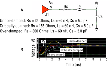
FIGURE 2. A series RLC circuit (a), and simulated response (Vr) to a step stimulus for under-damped, critically damped and over-damped cases (b).
|
These simulations were carried out using Mentor Graphics HyperLynx V7.5. The topologies were produced in the free form, as opposed to cell-based, style, which displays a more clear view of the circuit.
A formula relating the overshoot (amount of output rises above steady-state voltage level) to Q (resonance parameter) is described by Johnson et al.10. The circuit Q equals ratio of energy stored to energy lost per radian of oscillation.
Let us explore the relation between Q and ringing via PSpice simulations as illustrated by Figure 3. Figure 3b displays the driving step Vs (of amplitude 3.3V and rise time 500 ps) and simulated Vr for Q = 2.74 and 10.95. It indicates that circuit's Q directly influences ringing.
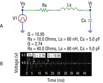
FIGURE 3. A series RLC circuit for analyzing Q variations (a), and simulated waveforms Vr to a step stimulus Vs for two Q values (b).
|
Lumped RLC modeling allows evaluation of ringing as demonstrated by Figure 3. Effects of varying inductance, capacitance, driver strength or output impedance can also be examined. Such analyses can reveal the need for altering load capacitance, trace impedance, flight time or incorporating termination. PCD&M
Dr. Abe (Abbas) Riazi is a senior staff electronic design scientist with ServerWorks (a Broadcom company) in Santa Clara, CA. He can be reached at This email address is being protected from spambots. You need JavaScript enabled to view it..
ACKNOWLEDGEMENTS
Thanks to Clement Yuen, Peter Arnold, Nasim Nirjhar and Victor Chow for reviewing the manuscript and providing valuable comments.
REFERENCES
1. Douglas Brooks, "Signal Integrity Issues and Printed Circuit Board Design", Prentice Hall, 2003, PP. 97-100, PP. 285-289.
2. IBIS (I/O Buffer Information Specification)", Version 4.1, January 30, 2004, PP. 12-13.
3. Abe Riazi, "Timing Analysis Principles for Digital PCBs, Part 1", Printed Circuit Design and Manufacture, April 2006, PP. 20-21.
4. Scott McMorrow and James Bell, " A Solution for the Design, Simulation and Validation of Board-to-Board Interconnects", High frequency Electronics, January 2005, PP. 18-28.
5. Jim Nadolny, "Cable Assembly Models for SPICE Simulation", Samtec Webinar, June 29, 2006.
6. Eoin McGibney and John Barrett, "An Overview of Electrical Characterization Techniques and Theory for IC Packages and Interconnects", IEEE Transactions on Advanced Packaging, Vol. 29, No.1, Feb 2006, PP. 131-139.
7. Wolfgang Maichen, "Easing the modeling of lossy lines", EDN, April 13, 2006, PP. 79-86.
8. Eric Bogatin, "Signal Integrity Simplified", Prentice Hall, 2004, P. 70, PP. 269-273, PP. 355-363.
9. Abe Riazi, "Via Modeling For High-Speed Simulations, Part 1", Printed Circuit Design and Manufacture, September 2003, P. 30.
10. Howard Johnson and Martin Graham, "High-speed Digital Design: A Handbook of Black Magic," Prentice Hall, 1993, PP. 134-136.
11. J.A. Coekin, "High-Speed Pulse Techniques," Pergamon Press, 1975, PP. 32-36.


