Not enough solder? Blame the via design!
Vias in pads can be “solder thirsty” and suck up solder from pads at terminals during reflow, creating what may appear to be solder insufficiency at the joints. This problem is typical of a via-in-pad design. It’s unpredictable as well; solder will randomly tend to fill those vias during the reflow process and some locations may appear worse than others, for example.
With a via-in-pad design, solder paste printed through an aperture of normal dimensions for the “toe” end of a pad at a rectangular end cap connection (FIGURE 1) may not provide enough solder during reflow to make a good solder fillet. The fillet may appear to be “starved,” because much of the solder that should be available to form a good solder joint will have wicked down the via and away from the end cap. The volume of solder lost will vary with the size and length of the via, the size of the component’s solderable surface(s) area, and other factors.
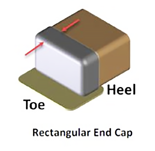
Figure 1. A rectangular end cap heel and toe.
There really is only one solution: provide more solder to replace that which is drawn off by the via. Adding that extra solder, by enlarging the print aperture on the toe side of the SMT pad by 35% (FIGURE 2), doesn’t do any harm, and is a quick fix because there will now be enough solder to satisfy the via’s “thirst” and form a good fillet.
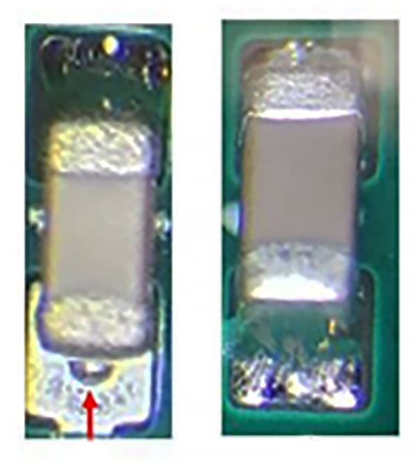
Figure 2. A stencil aperture of 1:1 (left) has left insufficient solder since it has been drawn off by the via (red arrow). On the right, a 35% increase in aperture area at the toe now provides enough solder to form a good solder joint.
Ultimately, if one cannot decide whether the amount of solder forming the fillet is sufficient, adhere to IPC-A-610 for correct guidance.
A via-in-pad design for passive components is never desirable unless the via is plugged. It’s preferable to route the via outside the SMT pad for passive components, of course, but sometimes space is an issue, so this is an alternate approach when the problem can’t be solved by design.

Figure 3. A normal 1:1 stencil aperture area (top), and on the bottom, an aperture area with the toe area of the SMT pad (yellow) increased by 35%.
With a greater volume of solder, depending on the application and alloy used, there are concerns that solder alloy brittleness could be a problem. To minimize such concerns, reflow at the correct temperature for the alloy and at the solder paste manufacturer’s profile recommendations.
Akber Roy is chief executive officer of Rush PCB Inc., a printed circuit design, fabrication and assembly company (rushpcb.com); This email address is being protected from spambots. You need JavaScript enabled to view it..


