As chiplet usage increases, chip-level concerns shift into the area of system-in-package implementation. Therefore, the system-in-package (SiP) must now accommodate electrical performance and cost considerations. A rapid prototyping tool flow that allows the engineering team to make quick assessments of these goals is essential.
Chiplets are emerging as a growing choice for product development. The main factor in this chiplet implementation growth is cost. Development costs for new chip designs on 5nm nodes could soar as high as $600 million. This rapid cost increase often leads companies to pursue more cost-efficient options. With the chiplet path, a company can leverage the higher performance chip technologies where it makes sense. It can then leverage lower technology fab capabilities where performance is less critical. For instance, a processor could be fabricated via 7nm, then the SRAM fabricated with a 14nm process. These tradeoffs permit the company to realize the most significant efficiencies for each element in its design.
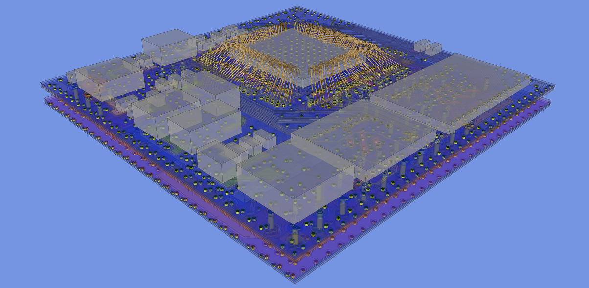
FIGURE 1. Example of a system-in-package (SiP) design.
When deciding to separate the chips at fabrication, engineering must then merge them on an SiP. This SiP becomes the critical merge point for these different functional elements. The SiP implementation must realize the signal and power integrity requirements while also monitoring the cost-efficiency of the SiP fabrication. Typically, evaluating a chosen chiplet and SiP configuration happens after completing significant design work, leading to a great deal of engineering effort. This design flow can also lead to lengthy process delays if targets are unattainable with the chosen configuration. When that happens, engineers must implement changes and restart the design cycle. These iterative cycles add time and, ultimately, increase costs.
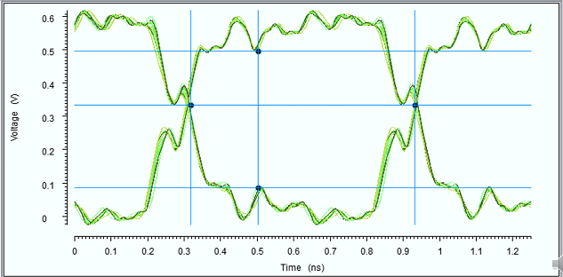
FIGURE 2. Waveform analysis of signals on the SiP.
Cost vs. performance.
Product development teams need the ability to design with decision speed and cost vs. performance requirements in mind. With such a design flow, they will have the option to bring the chiplet bump pattern into the equation to configure the most routable and highest performance redistribution layer arrangement. At the same time, they can also factor in the SiP-level routability of the bump arrangement. Of course, if the chiplet configuration is already fixed, the customer can leverage the SiP implementation flow for evaluations of various SiP configurations. These SiP configurations can include stacked die or through silicon via interposers if needed.
Speeding the evaluation process.
In partnership with a customer, we performed an evaluation of two different bump patterns for a prototype chiplet using the following process:
- First, using a partial array of these patterns, we placed those to die onto a SiP.
- Next, we examined the chiplet routing at the SiP level, focusing on routing length and signal integrity values. Through this examination at the SiP level, we determined that one configuration showed improvement over the other in length and signal quality.
- Third, we implemented the preferred configuration on the chiplet and incorporated it into the SiP.
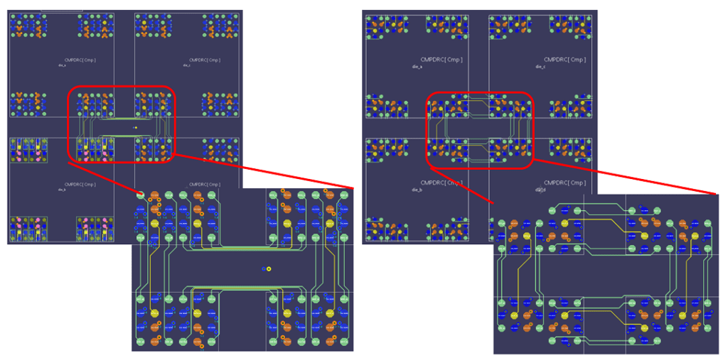
FIGURE 3. SiP-level routing of the two different configurations under consideration.
This new evaluation process allowed the customer to quickly converge on a design configuration that met the targeted goals. Further, it eliminated the need to evaluate the characteristics after considerable work on the final design. In the end, the process helped the customer avoid scheduling delays, and the electrical performance exceeded targeted goals.
These results bear a direct relationship too quickly evaluating various chiplet and SiP configurations and incorporating those results into the finalized design.
Steve Watt is manager of engineering operations, SOZO Center at Zuken USA (zukenusa.com); This email address is being protected from spambots. You need JavaScript enabled to view it..


